EN
EN
 it
it  fr
fr  de
de  ru
ru  pt
pt  es
es
Get in Touch with WeiYuanDa Now!


When circuit boards must carry currents above 10A continuously — in solar inverters, EV motor controllers, charger, industrial servo drivers, or server power supplies — standard 1 oz copper traces cannot keep up. Trace overheating, voltage drops, solder joint fatigue, and field failures become inevitable. Heavy copper PCBs solve this by using copper layers from 3 oz up to 10 oz (105–350 µm), transforming the board itself into a high-current pathway with integrated thermal dissipation.
This guide covers the core principles of heavy copper PCB design, manufacturing constraints that affect your layout choices, real-world application cases, and how WeiYuanDa (WYD) — with 20+ years of power electronics board production and UL-certified heavy copper capability up to 6 oz finished copper (210 µm) on inner and outer layers — approaches these challenges in practice. All specifications and process data referenced here are drawn from our actual production capabilities.
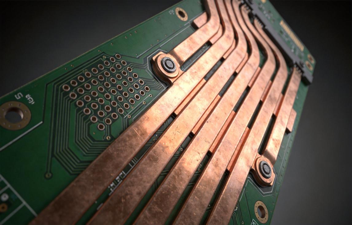
A heavy copper PCB is classified by its copper layer thickness exceeding 3 oz/ft² (approximately 105 µm). At WeiYuanDa, our heavy copper boards span 3 oz to 6 oz copper thickness (with UL certificated), built on FR-4 substrate with ENIG or OSP surface finish. This is fundamentally different from standard boards — the additional copper mass changes the electrical resistance, thermal dissipation path, and mechanical behavior of the entire structure.
WYD supports three structural configurations for heavy copper designs:
◆ Single-sided heavy copper — for straightforward high-current distribution boards
◆ Double-sided heavy copper — when both sides require significant current paths
◆ Multilayers heavy copper — combining power layers with signal routing layers in complex systems
The choice between these configurations depends on routing density, thermal budget, and system architecture. Our engineering team reviews Gerber files within 6 hours and provides DFM feedback on copper weight allocation, layer assignment, and via strategy before production begins.
Specification | WeiYuanDa Capability |
Copper Thickness | 3 oz – 6 oz per layer |
Base Substrate | FR-4 (high-Tg grades) |
Surface Finish | ENIG, OSP |
Thermal Conductivity (Copper) | ~401 W/m·K |
Board Structures Supported | Single-sided, Double-sided, Multilayer |
UL Certification (Heavy Copper) | Up to 6 oz finished copper (210 µm), inner & outer layers |
Etching Precision | Trapezoidal profile control with compensation algorithms |
Step Plating | Supported for selective thickness reinforcement |
Current Carrying Capacity
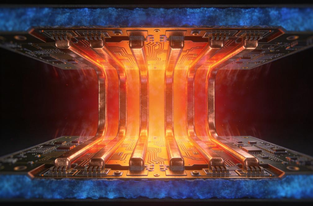
Copper's electrical resistance is inversely proportional to cross-sectional area. A 4 oz trace carries approximately four times the current of a 1 oz trace at the same width.
Thermal Performance
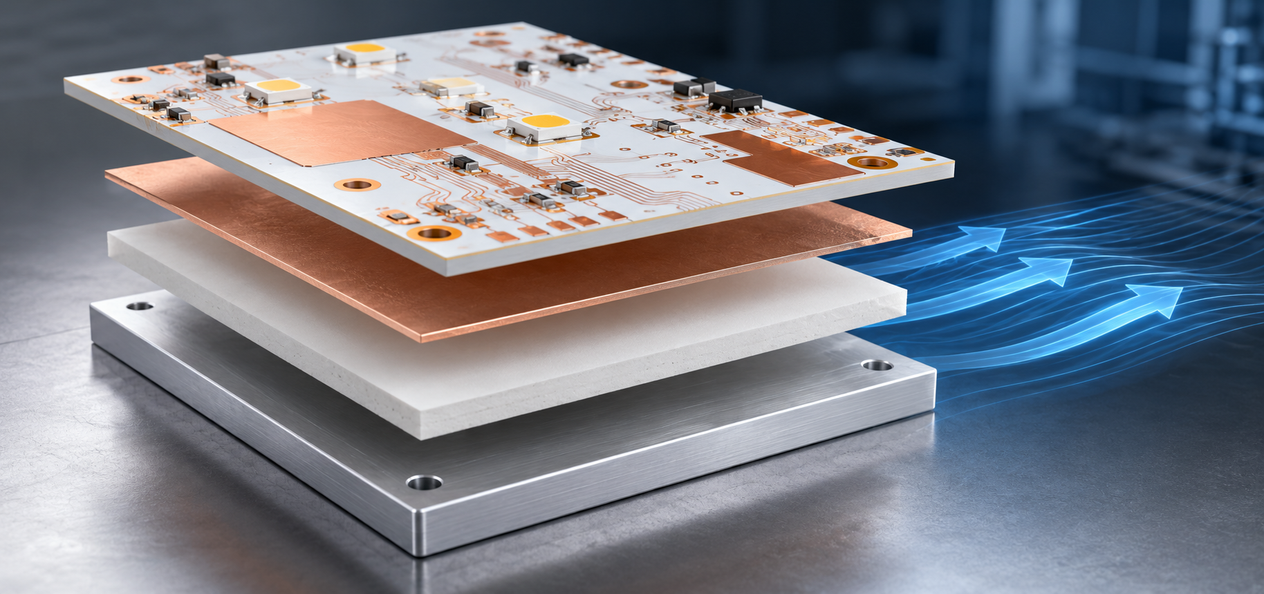
With thermal conductivity around 401 W/m·K, heavy copper layers serve as built-in heat spreaders. Thermal energy from power components — MOSFETs, diodes, inductors — is pulled away from pads and distributed across the copper plane. This reduces hotspot temperatures and extends component life. In applications like LED drivers and motor controllers, this often eliminates external heatsinks entirely.
Mechanical Stability Under Thermal Stress
In environments with rapid temperature swings — automotive under-hood installations, outdoor power equipment, industrial machinery — thick copper layers resist thermal cycling fatigue. Standard 1 oz traces can develop micro-cracks at solder joints over thousands of cycles. Heavy copper's additional mass provides structural stability that withstands these conditions, which is why WYD's IATF 16949 certification specifically supports automotive-grade heavy copper production.
Simplified System Architecture
By embedding current carrying and heat dissipation directly into the PCB, heavy copper designs reduce the need for supplementary components — fewer bus bars, heatsinks, and cooling fans. This design efficiency is particularly valuable in compact enclosures for power modules and EV subsystems where board space is at a premium.
Manufacturing Challenges and WYD's Process Solutions
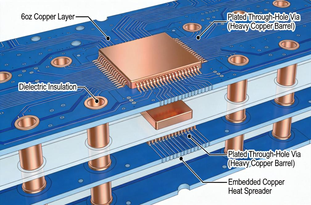
Heavy copper fabrication is not simply a matter of using thicker copper foil. The increased copper thickness introduces manufacturing challenges that require specialized process controls.
Etching Precision
As copper thickness increases, etching must remove more material while preserving accurate trace geometry. Standard etching produces excessive undercut on thick copper, creating trapezoidal profiles that deviate from design intent. WYD's etching process uses compensation algorithms calibrated for 3–10 oz copper, maintaining line width accuracy even on boards with mixed-weight copper areas.
Step Plating for Selective Reinforcement
For copper weights above 4 oz, most manufacturers cannot plate the full thickness in a single pass. At WYD, we use step plating or Copper strip — building copper in stages with intermediate etching steps. This allows selective thickness reinforcement in high-current zones while maintaining finer geometry in signal regions. Step plating requires close coordination between design engineers and the fab team, and WYD's 24+ engineers work along with the our Sales Representative directly with clients to optimize the layer build-up sequence.
Dielectric Fill and Lamination Control
Thicker copper traces create taller profile differences between copper and substrate. The dielectric material must fill these gaps completely to prevent voids that could cause insulation breakdown. WYD controls lamination pressure and temperature profiles to ensure consistent dielectric fill — this is especially critical for multilayers heavy copper constructions where multiple thick copper layers are stacked together.
UL Certification and Quality Verification
WYD's heavy copper PCBs carry UL certification for inner and outer layers up to 6 oz finished copper thickness (based on 175 µm base copper plus 35 µm plating), certified for both US and Canada markets. Every board undergoes AOI trace verification, microsection analysis after Thermal Stress for copper thickness and via integrity.
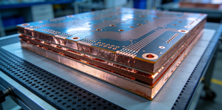
Heavy copper technology is not needed for every design. Low-power signal boards work perfectly on standard Hoz or 1 oz copper. But for the following applications, heavy copper is often the only practical choice — and these are the sectors where WYD has accumulated the deepest production experience:
Automotive and Electric Vehicles: EV battery management systems, motor drive controllers, and onboard chargers operate under constant thermal and vibration stress. WYD's IATF 16949 certification ensures automotive-grade quality for boards operating across -40°C to 125°C and beyond.
Industrial Control and Automation: Welding equipment, servo controllers, and power distribution boards demand PCBs that handle sustained high currents without degradation. Heavy copper's thermal stability reduces maintenance intervals and unplanned downtime.
Renewable Energy: Solar inverters and wind power converters face fluctuating loads in harsh outdoor conditions. Heavy copper manages high-current DC/AC paths while dissipating heat efficiently — delivering higher conversion efficiency in installations where maintenance access is limited.
Aerospace and Defense: Flight-critical power modules require absolute reliability. The combination of FR-4 substrate stability and thick copper construction meets stringent aerospace environmental requirements, with WYD's ISO 13485 and ISO 9001 certifications supporting quality traceability for these applications.
Founded in Hong Kong with a dedicated manufacturing base in Dongguan, WeiYuanDa (WYD) has been building printed circuit boards for more than two decades. Our 12,000 m² facility delivers over 4,000 part numbers every month to engineering teams and procurement departments across more than 50 countries world-wide.
Rather than covering a narrow segment, we maintain capability across the full PCB technology spectrum — from standard multilayer FR-4 and HDI boards to high-frequency laminates, heavy copper power carriers, and aluminum-based thermal designs. This breadth allows us to address the diverse needs of automotive, industrial automation, telecom, IoT, energy supply, and lighting programs without requiring our customers to qualify multiple vendors.
Every batch passes through the same inspection standards regardless of order size. Our certifications — ISO 9001, ISO 14001, ISO 13485, IATF 16949, and UL for both the US and Canada — are validated across the entire product range. Prototype runs and mass production share identical process controls, which means the board you approve on day one is the same board you receive on order number ten thousand.
Engineering inquiries receive a quotation within two hours, backed by round-the-clock technical support from our teams based across China and Italy. Whether your program requires a single prototype or a recurring monthly schedule, WYD is structured to respond with the speed and consistency your timeline demands.
Heavy copper PCB technology transforms the board from a simple electrical interconnect into an integrated power delivery and thermal management platform. Choosing the right copper weight, understanding manufacturing constraints, and partnering with an experienced fabricator are the three factors that determine whether your heavy copper design performs reliably in the field.
Whether you are prototyping a next-generation EV battery management system or scaling production of industrial power modules, WeiYuanDa's 20+ years of heavy copper expertise, UL certification, and full-cycle manufacturing capability make us a partner you can rely on from first prototype through volume production.
Q1: What copper weight range does WYD support for heavy copper PCB?
A1: WYD supports copper thickness from 3 oz up to 10 oz per layer, with UL certification for finished copper up to 6 oz (210 µm) on both inner and outer layers.
Q2: Can heavy copper PCBs be built as multilayer boards?
A2: Yes. WYD produces single-sided, double-sided, and multilayer heavy copper configurations. Multilayer designs require specialized step plating and lamination control to maintain dielectric fill and trace definition.
Q3: What surface finishes are available for heavy copper boards?
A3: WYD offers ENIG and OSP as standard surface finishes for heavy copper PCBs, selected based on soldering process, environmental requirements, and shelf-life expectations.
◆ Email: wai.tsang@microstar-pcb.cn
◆ Phone: +852 6941 6654 / +86 136 0252 7201
◆ Address: The 4th Industrial Zone, Nance, Humen, Dongguan, Guangdong, China
◆ Website: www.wyd-pcb.com