EN
EN
 it
it  fr
fr  de
de  ru
ru
Get in Touch with WeiYuanDa Now!


Meta Description: Discover how HDI PCB technology solves critical 5G base station challenges — high-frequency signal integrity at 28GHz+ and thermal management in compact designs. Learn about materials, microvias, and manufacturing expertise from WeiYuanDa PCB.

When we stream 4K video on our phones or experience sub-millisecond latency in autonomous vehicles, we rarely think about what makes it all possible. The answer lies not just in the towering 5G base stations we see on rooftops and hillsides, but deep inside them — on a piece of technology smaller than your hand: the High-Density Interconnect (HDI) PCB.
5G networks operate at frequencies far beyond anything previous generations used. Sub-6 GHz bands and millimeter-wave (mmWave) spectrum at 28 GHz and 39 GHz demand a fundamental rethinking of how printed circuit boards are designed, manufactured, and deployed. The challenges are twofold: maintaining signal integrity at extremely high frequencies while simultaneously managing heat dissipation in increasingly compact, power-dense modules.
Specialized manufacturers such as WeiYuanDa Industrial Co., Limited are the ideal solution here. With more than 20 years of accumulated expertise in PCB production, our company has developed manufacturing technologies optimised for highly complex and high-frequency applications.
High-Density Interconnect PCBs are not simply “more layers crammed together.” According to the IPC-2226 standard, HDI boards are defined by specific structural characteristics that set them apart:
Feature | Conventional PCB | HDI PCB |
Trace Width/Spacing | ≥ 6 mil (150 μm) | 2–4 mil (50–100 μm) |
Via Structure | Mechanical through-hole | Laser-drilled microvia (≤ 0.15 mm) |
Dielectric Thickness | ≥ 4 mil (100 μm) | 1–2 mil (25–50 μm) |
Routing Density | Baseline | 3× higher than conventional |
Layer Count Reduction | N/A | 30–40% fewer layers for equivalent functionality |
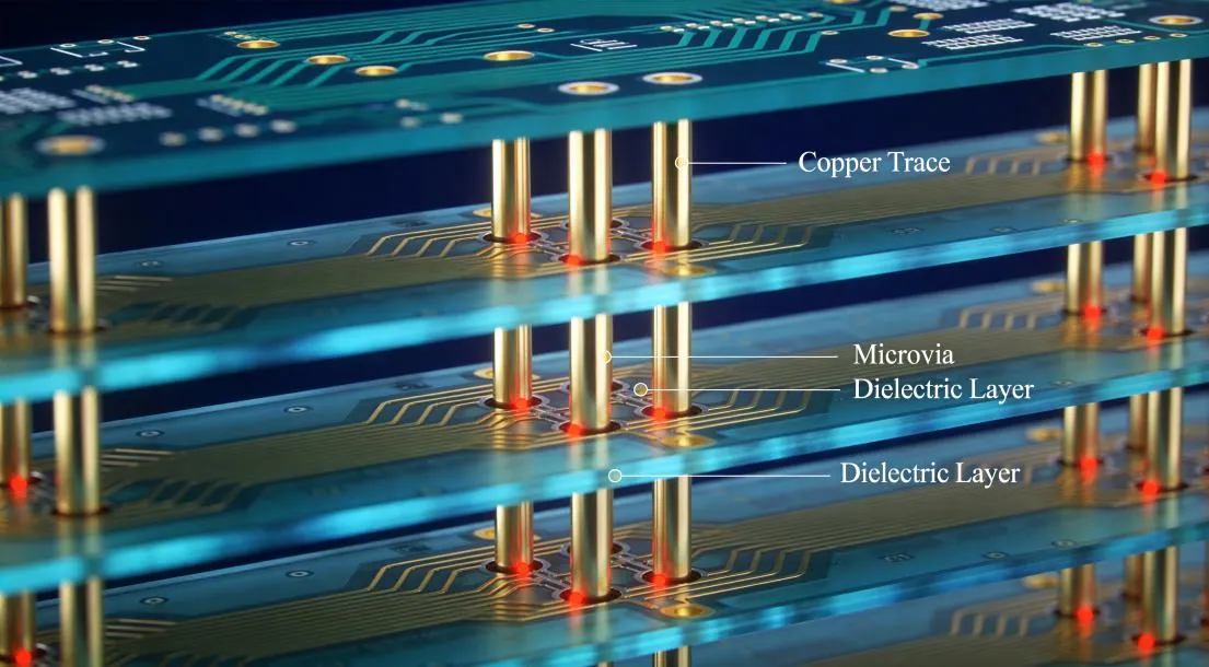
The core advantage is derived from microvia technology. These laser-drilled holes feature a diameter below 0.15 mm and an aspect ratio of 1:1, enabling interlayer connections which cannot be realised using conventional mechanical drilling processes.
This yields shorter signal transmission paths alongside considerably lower parasitic inductance – reaching merely one tenth of the inductance value exhibited by through-hole vias. Furthermore, this technology facilitates the integration of fine-pitch components such as BGA assemblies with a pitch of 0.25 mm.
5G base stations equipped with 64T64R Massive MIMO antenna arrays require 240 antenna feed lines to be routed on a single PCB.
This layout achieves a density of eight differential pairs per square centimetre, which is four times the routing density of typical 4G circuit designs.
At such high packing densities, crosstalk between adjacent conductor tracks may deteriorate from -60 dB down to -45 dB, breaching the limit value of -55 dB defined in official 5G specifications.
HDI technology mitigates this issue via the following measures:
• Dedicated reference ground planes assigned to each individual signal layer, reducing crosstalk by up to 92 %
• Staggered microvia structures implemented in place of stacked vias, cutting parasitic inductance by 58 %
• Ground shielding vias arranged around signal vias at defined regular intervals
A signal attenuation of roughly 15 dB occurs across a 10 cm conductor track manufactured from standard FR-4 base material at 28 GHz; this attenuation level is ten times higher than that measured at the 2 GHz operating frequency used for 4G networks.
Material selection consequently represents one of the most decisive design considerations for 5G HDI PCB development.
Established manufacturers such as WeiYuanDa supply hybrid laminate stack-up configurations: low-loss substrates including Rogers RO4350B (Dk = 3.48, Df = 0.0031) are used for high-speed signal layers, while standard FR-4 material is adopted for power supply layers and structural support layers.
This material combination reduces overall material expenditure by 30–45 %, while fully satisfying the signal performance requirements imposed by mmWave applications.
5G base station components generate three times the power density of their 4G counterparts — approximately 30 W/cm² versus 10 W/cm². Power amplifier (PA) modules, in particular, generate concentrated heat that must be dissipated efficiently to prevent thermal throttling and premature component failure.
The challenge is compounded by HDI’s very architecture: microvias (0.1 mm) and fine traces (0.08 mm) impede thermal conductivity, creating thermal resistance of up to 20°C/W compared to 10°C/W for conventional PCBs. Without proper thermal design, chip temperatures can rise 15°C above 4G baselines, requiring additional heatsinks that add 20% to module volume.
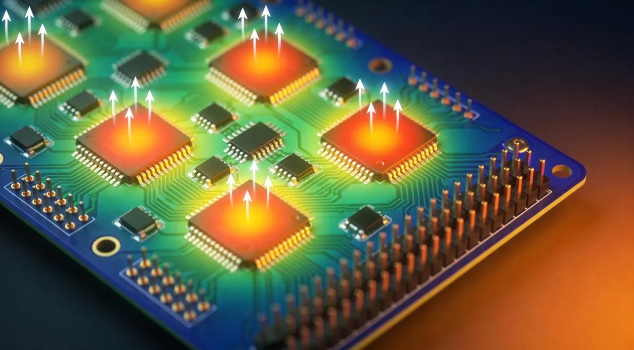
Modern 5G HDI PCBs employ several thermal management techniques:
Copper-Filled Stacked Microvias (CFSM): By fully filling each microvia with electroplated copper before stacking the next layer, thermal conductivity reaches 35–40 W/m·K — providing a direct heat path from chip to board. WeiYuanDa’s manufacturing process achieves >99.8% via-fill reliability through controlled lamination and plating.
Heavy Copper Integration: For power-intensive sections, incorporating heavy copper layers (3 oz to 20 oz) dramatically improves current-carrying capacity and heat spreading. WeiYuanDa’s expertise in Heavy Copper PCB manufacturing makes them particularly well-suited for 5G PA modules and power management sections.
Metal Core and Aluminum Substrates: In sealed outdoor enclosures where forced air cooling isn’t available, Aluminum PCBs provide thermal conductivity 5–10 times that of standard FR-4, making them ideal for 5G remote radio units (RRUs).
Thermal Via Arrays: Strategic placement of thermal vias beneath hot components creates vertical heat pipes that channel heat to inner ground planes or bottom-side heat sinks.
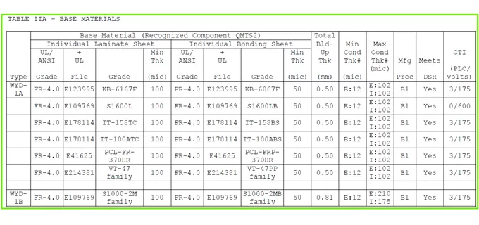
The choice of substrate material fundamentally determines an HDI board’s high-frequency performance. Here’s how different materials compare for 5G applications:
WeiYuanDa maintains a large inventory of Rogers materials and high-performance FR-4 laminates, enabling rapid prototyping for time-sensitive 5G development projects. Their Dongguan facility’s sequential lamination process ensures precise layer-to-layer alignment — critical for maintaining the ±3% impedance tolerance that 5G HDI designs require.
When it comes to 5G HDI PCBs, the gap between design intent and manufactured reality is where many projects fail. This is precisely where an experienced manufacturing partner makes all the difference.
Two Decades of Specialized Expertise
Founded in 2005 and headquartered in Hong Kong with a production facility in Dongguan, China, WeiYuanDa Industrial Co., Limited has built its reputation on exactly the type of complex, high-difficulty PCBs that 5G infrastructure demands. Their product portfolio spans HDI PCBs up to 32 layers, high-frequency boards, and heavy copper solutions — the three pillars of 5G base station electronics.
What sets WYD apart in the 5G context:
Rapid Prototyping: Single-layer prototypes in 24 hours, RFQ responses within 2 hours — critical for the fast iteration cycles of 5G module development.
Certification Depth: ISO 9001, ISO 14001, ISO 13485 (medical), IATF 16949 (automotive), and UL certifications — meaning their quality systems meet the stringent requirements of telecom OEMs across global markets.
European Local Support: Their Italy-based subsidiary provides direct technical support and customer service for European clients — a significant advantage when you consider that many of the world’s leading telecom equipment manufacturers are based in Europe.
Direct Manufacturer Advantage: As a factory-direct supplier with no intermediaries, WeiYuanDa offers engineering-level communication with their 24+ engineer team, ensuring that design-for-manufacturing feedback reaches clients quickly.
Their advanced HDI capability — supporting up to 32 layers with 2 mil line/space and 0.10 mm laser vias — directly addresses the density and precision requirements of 5G AAU (Active Antenna Unit) and BBU (Baseband Unit) designs.
While 5G deployment is still in full swing, the PCB industry is already looking ahead to 6G, which will operate in the terahertz range (100 GHz–300 GHz). This will push HDI technology even further:
Sub-25 μm line/space will become standard (current advanced HDI achieves 50 μm)
Any-layer HDI with full copper-filled stacked vias will be mandatory for the routing density required
New substrate materials — including ceramic-polymer hybrids and glass-based substrates — will replace traditional laminates
AI-driven design optimization will be needed to manage the exponentially increasing complexity of signal integrity, thermal, and electromagnetic compatibility constraints
Manufacturers investing in R&D today — like WeiYuanDa’s Dongguan R&D lab developing microvia and heavy copper innovations — will be the ones ready when 6G arrives.
HDI PCBs are the unsung heroes of the 5G revolution. Without the microvia technology, ultra-fine routing, and thermal management strategies they enable, the high-frequency, high-density, high-power requirements of 5G base stations would simply be impossible to meet.
For engineering teams designing 5G infrastructure, choosing the right PCB manufacturing partner is as important as the design itself. A partner who understands signal integrity at 28 GHz, who can deliver copper-filled microvias with >99% reliability, and who offers the material expertise and certification depth that telecom OEMs demand.
WeiYuanDa PCB has spent 20 years building exactly this capability. From their Dongguan production facility to their European office in Italy, from rapid prototyping to full-scale production, they provide the manufacturing expertise that turns 5G design ambition into deployed reality.
To learn more about HDI PCB capabilities or request a quote for your 5G project, visit www.wyd-pcb.com or contact their engineering team at wai.tsang@microstar-pcb.cn.
Q1: What is an HDI PCB, and why is it critical for 5G?
A: HDI (High-Density Interconnect) PCBs utilize laser-drilled microvias, ultra-fine traces, and thin dielectric layers to achieve routing densities 3–5× higher than conventional PCBs. For 5G base stations operating at 28 GHz and above, this translates into shorter signal paths, lower insertion loss, and superior impedance control—all essential for reliable mmWave performance.
Q2: How does HDI PCB technology manage thermal loads in 5G equipment?
A: 5G HDI boards employ copper-filled stacked microvias (achieving 35–40 W/m·K thermal conductivity), heavy copper layers, aluminum substrates, and strategic thermal via arrays to efficiently dissipate heat from power-dense components, such as power amplifiers.
Q3: What are the lead times for HDI prototypes?
A: Specialized manufacturers like WeiYuanDa can deliver single-layer prototypes within 24 hours, with RFQ responses provided within 2 hours. Complex multi-layer HDI prototypes typically require 5–12 days, depending on the layer count and material availability.