EN
EN
 it
it  fr
fr  de
de  ru
ru  pt
pt  es
es
Get in Touch with WeiYuanDa Now!


Quick Answer: A standard aluminum PCB stack-up uses a copper circuit layer, a thermally conductive dielectric, and an aluminum base. The stack-up must balance current carrying, heat transfer, electrical isolation, mechanical stiffness, manufacturability, and cost.
An aluminum board can look simple from the outside, yet small changes in copper weight, dielectric thickness, material grade, or core thickness can produce large differences in temperature, voltage isolation, flatness, and assembly behavior.
This guide explains each layer, compares common constructions, and provides a practical specification checklist for LED, automotive, industrial, and power-electronics projects.
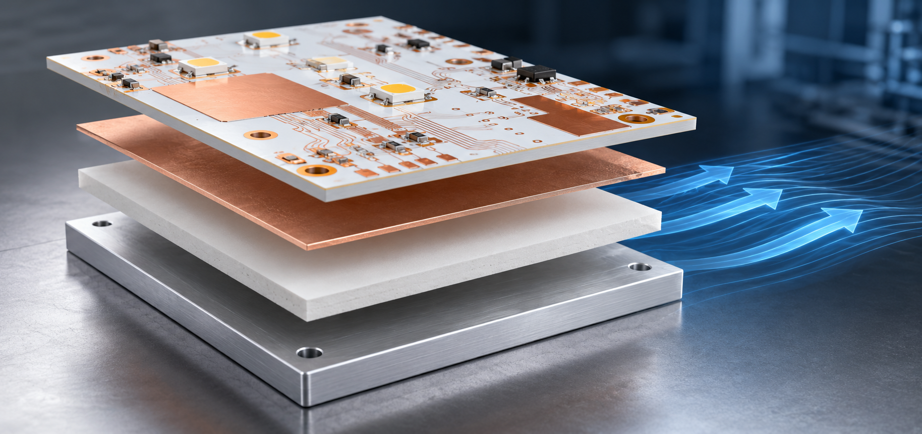
The basic single-layer construction consists of solder mask and legend over a patterned copper circuit, a thermally conductive electrical insulation layer, and an aluminum base.
The copper carries signals and current and also spreads heat across the board surface. The dielectric bonds the circuit to the metal core, isolates the copper electrically, and transfers heat vertically. The aluminum base provides mechanical support and distributes heat into the enclosure or heat sink.
This construction is commonly called an aluminum core PCB or metal core PCB. It is widely used when a conventional organic laminate cannot move heat efficiently enough from LEDs or power components.
The copper layer must be sized for electrical current, voltage drop, thermal spreading, etching capability, and component-pad geometry.
Higher copper weight can support higher current and improve lateral heat distribution, but it also changes etching compensation, minimum line and spacing, pad definition, and cost. Local copper neck-downs near terminals or power components may become hot even when the average copper coverage is large.
For a custom aluminum PCB, the copper pattern should be reviewed together with the thermal map. WYD’s aluminum PCB manufacturing page can be used to discuss available copper, thickness, finish, and prototype options.
The aluminum PCB dielectric layer is usually the most important layer because it must provide electrical insulation and thermal transfer at the same time.
A thinner dielectric generally lowers thermal resistance, but the minimum practical thickness depends on material construction, copper topography, working voltage, surge conditions, test voltage, and manufacturing tolerance. A high-conductivity material is useful only when its data is tied to a specific grade and test method.
Engineers should specify the required dielectric strength and thermal target rather than asking for the thinnest possible layer. The fabricator can then recommend a material that provides a repeatable process window.
The aluminum base controls stiffness, flatness, mass, heat spreading, machining behavior, and the mechanical connection to the final product.
Thin cores reduce weight and fit compact assemblies, while thicker cores resist warpage and provide a stronger platform for large boards, heavy connectors, or vibration. The best choice depends on board dimensions, mounting points, cutouts, depaneling method, enclosure design, and thermal interface area.
Alloy selection can influence strength, machinability, surface quality, and supply availability. It should be treated as part of the mechanical specification rather than selected only by its bulk conductivity.
Single-layer boards provide the simplest heat path and are the most common aluminum construction, while double-layer and multilayer versions add routing density at the cost of a more complex insulation and interconnection structure.
Construction | Best Fit | Main Advantages | Key Design Risks |
Single-layer aluminum PCB | LED modules, power conversion, automotive lamps, motor-control subcircuits | Direct heat path, lower cost, easier thermal modeling | Limited routing density and one copper circuit layer |
Double-layer aluminum PCB | Moderate routing density with metal-base cooling | More routing flexibility and plated interconnection options | More complex dielectric structure, via isolation and process control |
Multilayer aluminum PCB | Compact high-function designs requiring metal-base heat spreading | Combines routing density with a metal heat-spreading layer | Higher cost, longer DFM review, complex thermal and isolation paths |
Copper-core or special metal-base PCB | Very high heat flux or specialized mechanical requirements | Potentially stronger heat spreading or mechanical performance | Material cost, weight, machining and supplier capability |
A lighting stack-up should prioritize uniform temperature, stable LED output, suitable solder mask, and reliable attachment to the luminaire body. The lighting PCB solution page is a useful internal reference for matching board construction to streetlights, automotive lighting, industrial fixtures, and commercial luminaires.
A power-electronics stack-up must additionally review current density, isolation, switching voltage, creepage and clearance, heavy terminals, and local semiconductor losses. Mechanical clamping and thermal interface pressure often deserve the same attention as the laminate specification.
Automotive and industrial designs should also consider thermal cycling, vibration, moisture exposure, connector load, and traceability requirements.
A complete RFQ allows the manufacturer to evaluate the electrical, thermal, and mechanical design before material is ordered.
· Gerber or ODB++ data, fabrication drawing and panel requirements.
· Board outline, thickness tolerance, aluminum thickness and preferred alloy if controlled.
· Copper weight, minimum line and spacing, finished hole sizes and surface finish.
· Dielectric material or required conductivity, thickness and dielectric strength.
· Working voltage, test voltage, creepage and clearance constraints.
· Component power map, maximum ambient temperature and cooling method.
· Flatness, machining, countersink, V-cut, routing and depaneling requirements.
· Prototype quantity, production forecast, inspection level and required reports.
Before release, request a DFM review of the complete stack-up. WYD PCB capability information outlines the inspection and fabrication resources that can support prototype and production evaluation.
The most common structure is copper circuit, thermal dielectric, and aluminum base, with solder mask and legend on the circuit side.
The dielectric frequently controls through-board thermal resistance because it must be electrically insulating and is much less conductive than the metal core.
Yes. Double-layer and multilayer metal-base structures are possible, but they require more complex insulation, via, lamination, and DFM control.
No. It can improve current capacity and spreading, but it may increase cost and reduce fine-feature capability. The copper should be matched to current, routing, thermal, and etching requirements.
The choice depends on board size, stiffness, mounting, vibration, weight, machining, and heat-spreading area. It should be selected with the enclosure and assembly design.
Send Gerber or ODB++, fabrication notes, board drawing, copper requirements, dielectric and voltage targets, power information, and the mechanical cooling concept.