EN
EN
 it
it  fr
fr  de
de  ru
ru  pt
pt  es
es
Get in Touch with WeiYuanDa Now!


High-density electronics require more than a PCB factory that can produce fine lines. Smartphones, IoT modules, medical electronics, AI devices, automotive systems, and telecom products often need microvias, blind vias, buried vias, via-in-pad structures, impedance control, and stable process documentation. For overseas customers, choosing an HDI PCB exporter also means checking communication, export experience, quality control, file review, and delivery response.
An HDI PCB project can fail early if stack-up feasibility, microvia structure, material selection, or surface finish is not reviewed before production. It can also fail later if quotation, engineering confirmation, inspection records, or logistics communication are not handled clearly.
This revised article focuses on exporter evaluation and international project handling, so it avoids repeating the technical definition and manufacturing-process article.
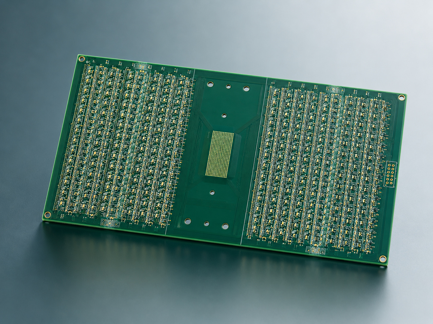
For overseas customers, the best HDI PCB exporter is not only a production source. The exporter should understand how to communicate with engineering teams, purchasing teams, EMS partners, and quality departments across different time zones. This is especially important when a project moves from prototype to small-batch production or repeat orders.
Export experience also affects how quickly questions are clarified. HDI projects may involve material alternatives, line/space checks, via filling requirements, impedance data, panelization, surface finish, and lead-time planning. If these points are not confirmed early, delivery and yield risk can increase.
Before confirming an HDI PCB exporter, customers should ask for practical capability information instead of accepting a general statement such as “we can make HDI boards.” The supplier should be able to explain microvia size, line/space capability, layer count, lamination structure, material options, and inspection process.
For high-density products, the key is not only whether the board can be made once, but whether the process can remain stable for follow-up production.
Capability item | Why it matters | Customer check point |
Microvias / laser drilling | Supports compact interconnection and high-density routing | Confirm via size, layer connection, filling requirement |
Blind and buried vias | Improves routing flexibility in limited space | Confirm stack-up and lamination sequence |
Fine line / spacing | Supports BGA and high-pin-count components | Check minimum line/space against design needs |
Via-in-pad process | Reduces routing distance under small packages | Confirm plugging, filling, plating, and surface flatness |
Inspection and testing | Controls reliability before shipment | Ask for AOI, flying probe, X-ray, impedance, and final inspection |
A clear quotation package helps the HDI PCB exporter review manufacturability faster. It also reduces repeated email communication and helps avoid misunderstanding between design, sourcing, and factory teams.
· Gerber files and drill files
· Layer stack-up target and material preference
· Microvia, blind via, buried via, or via-in-pad requirements
· Line width, spacing, copper thickness, and impedance requirements
· Surface finish such as ENIG, OSP, HASL-LF, immersion tin, or gold finger
· Quantity, delivery expectation, application industry, and quality requirement
HDI boards usually need more pre-production clarification than standard FR-4 boards. A good exporter should not simply reply with a price. The engineering team should review whether the design can be produced consistently and should point out risks such as too-aggressive line spacing, difficult via filling, unsuitable material, or stack-up imbalance.
Customers should also check whether the supplier can support prototype feedback, revision management, and production planning. This is important for overseas OEM and EMS projects where design changes may continue after the first sample run.
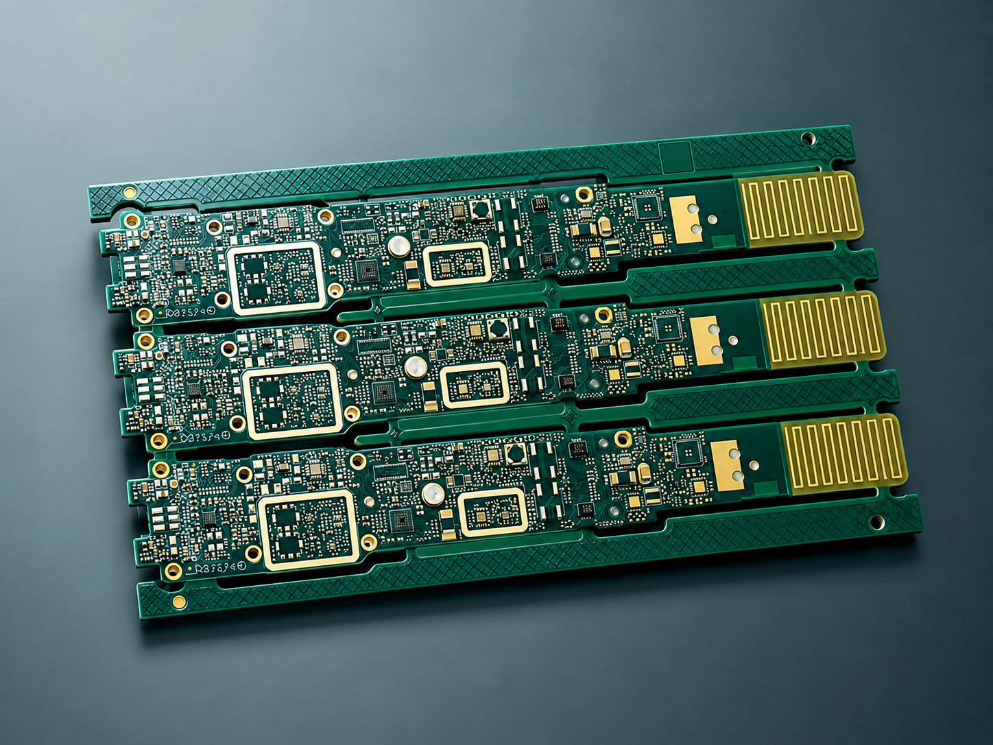
Quality control for HDI PCB should cover incoming material control, laser drilling accuracy, plating quality, lamination registration, surface finish, electrical testing, and final inspection. For compact devices, small defects may affect assembly yield or field reliability.
Inspection equipment such as AOI, X-ray inspection, impedance testing, and flying probe testing can help verify that production meets design requirements. Customers can also ask whether inspection records, test reports, or project-specific quality documentation are available when needed.
WEIYUANDA PCB has more than 20 years of PCB manufacturing experience and supports Multilayer HDI PCB, High-Frequency PCB, and IMS PCB projects. For HDI PCB projects, customers can share stack-up requirements, Gerber files, material preferences, impedance needs, surface finish requirements, production volume, and delivery targets for engineering review.
The company emphasizes quality control, on-time delivery, and fast response, which are important for overseas customers who need reliable communication from prototype evaluation to repeat production.
View WEIYUANDA HDI PCB manufacturing capabilities or contact the WEIYUANDA PCB team for project review and quotation support.
Choosing an HDI PCB exporter in China should not be based only on price. Customers should evaluate engineering response, microvia capability, stack-up review, material knowledge, inspection process, export communication, and delivery planning.
For high-density electronics, a reliable exporter can help reduce design risk, improve prototype feedback, and support a smoother transition to production.