EN
EN
 it
it  fr
fr  de
de  ru
ru  pt
pt  es
es
Get in Touch with WeiYuanDa Now!


As electronic devices shrink in size while demanding higher processing power, faster data rates, and more complex functionality, single-sided and double-sided PCBs reach their limits. Dense BGA components, high-speed memory interfaces, mixed-signal architectures, and multi-rail power distribution all require the routing density and signal isolation that only multilayer PCB structures can deliver. WeiYuanDa (WYD), with 20+ years of multilayer fabrication experience and monthly output of 4,000 part numbers, serves as a trusted manufacturing partner for global OEMs needing both rapid prototypes and scalable mass production of complex multilayer boards.
This technical guide — compiled by our in-house engineering team — walks through multilayer PCB architecture fundamentals, critical stack-up design principles, manufacturing process challenges, industry application cases, and the full set of proprietary fabrication capabilities available at WYD. We draw on two decades of experience manufacturing boards up to 40 layers to explain how precise process control solves common design pitfalls for clients across 50+ countries.
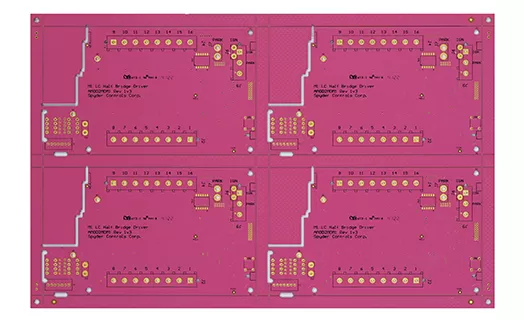
A multilayer PCB consists of three or more conductive copper layers laminated together with insulating prepreg and core materials, interconnected through precision-engineered vias. Unlike basic double-sided boards where all routing competes for just two copper planes, multilayer structures dedicate separate layers to specific functions — signal routing, power distribution, and ground return — creating a highly organized electrical architecture.
Signal, Power, and Ground Layer Assignment
Effective multilayer design begins with assigning each copper layer a clear role. High-speed signal traces are routed adjacent to solid ground planes to establish controlled impedance return paths. Dedicated power planes distribute voltage rails with minimal impedance, while inner signal layers handle secondary routing without competing for surface space. This layered approach is what enables modern boards to pack thousands of components into compact form factors.
Via Types and Interconnection Architecture
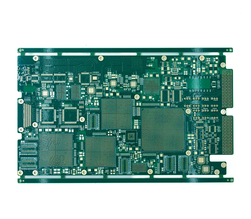
Three via types create electrical connections between layers. Through-holes pass through the entire board stack and are the simplest to manufacture. Blind vias connect an outer layer to one or more inner layers without penetrating the full thickness. Buried vias connect inner layers only and are invisible from either board surface. Advanced HDI designs combine all three via types — some WYD boards utilize through-holes, blind vias, and microvias in a single stack-up to achieve maximum routing density within tight space constraints.
Material and Tg Selection
The insulating layers between copper planes determine the board's thermal endurance, mechanical stability, and electrical performance. WeiYuanDa supports Tg options ranging from TG135 to TG280, allowing engineers to match material properties to their application's thermal environment. High-Tg materials resist deformation during lead-free soldering reflow cycles and maintain dimensional stability across operating temperature ranges — critical for automotive, telecom and industrial aerospace applications.
Stack-up Design Principles That Prevent Signal Integrity Failures
A poorly planned layer stack-up is the root cause of most multilayer PCB problems — impedance mismatches, crosstalk between adjacent layers, excessive board warpage, and thermal delamination during assembly. The following principles guide every stack-up we engineer at WYD.
Symmetric Stack-up for Warpage Prevention
Balancing copper distribution above and below the board's central axis prevents warpage during thermal cycling and reflow soldering. An asymmetric stack creates unequal thermal expansion forces that bend the board — potentially cracking solder joints or damaging components. Our engineering team always validates stack-up symmetry before proceeding to lamination.
Controlled Impedance Routing
High-speed digital and RF circuits require precise trace impedance — typically 50Ω single-ended or 100Ω differential. Trace width, dielectric thickness, copper thickness, and Dk value all influence impedance. WYD maintains ±10% impedance tolerance on standard designs and ±8% on advanced HDI boards, verified through TDR (Time Domain Reflectometry) testing on every production panel.
Decoupling Capacitor Placement and Plane Continuity
Continuous ground and power planes provide low-impedance return paths for high-frequency currents. Split planes or gaps beneath high-speed traces force return currents to take longer detour paths, creating EMI radiation and signal degradation. Our DFM review process flags plane discontinuities and recommends via stitching patterns to maintain uninterrupted ground reference.
Manufacturing Process: From Inner Layer Etching to Final Inspection
Multilayer PCB fabrication involves a precise sequence of processes, each introducing variables that directly affect board quality. Understanding this workflow helps engineers set realistic design expectations.
Inner Layer Imaging and Etching
Each inner copper layer is patterned using high-resolution imaging and precision etching. WYD achieves minimum line/space of 3 mils on standard designs and 2 mils on advanced HDI boards. Automated Optical Inspection (AOI) verifies every inner layer before lamination — catching defects early prevents costly scrap after the board is pressed together.
Lamination and Drill Processing
Inspected inner layers by AOI scan are stacked with prepreg sheets along with outer copper foil, then laminated under precisely controlled heat and pressure.
After lamination, through-holes and via pads are drilled — WYD supports minimum drill diameters of 0.15mm (standard) and 0.10mm (advanced HDI). For high-speed designs, back drilling removes via stubs to eliminate signal reflections, with capability for up to 6 back drill cycles on complex boards.
Plating, Surface Finish, and Outer Processing
Drilled holes are copper-plated to establish electrical connections between layers. Outer layers are then imaged, etched, and finished with the specified surface treatment. WYD supports HASL-LF, ENIG, ENPIG, OSP, immersion tin, immersion silver, and gold finger plating — selected based on application requirements for solderability, wire bonding, or edge connector durability.
Electrical Testing and Reliability Validation
Every completed board undergoes 100% electrical testing either by fly probe or E-Test Fixture to verify connectivity and isolation. Impedance measurements confirm trace geometry accuracy, microsection analysis validates plating quality and via integrity, and thermal shock testing confirms material bonding strength before shipment.
Below is WeiYuanDa's complete multilayer PCB manufacturing capability range:
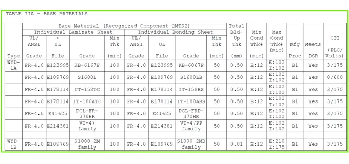
| Parameter | Standard (With UL) | Advanced HDI |
| Layer Count | Up to 24 Layers | Up to 40 Layers |
| Max Delivery Size | 950mm x 600mm | 1200mm x 600mm |
| Tg Options | TG135/TG150/TG170/TG180 | Same |
| Max Board Thickness | 5.0mm | Same |
| Outer Base Copper | Up to 8OZ | Up to 100Z |
| Inner Base Copper | Up to 6OZ | Up to 8OZ |
| Aspect Ratio | 12:1 | 15:1 |
| Min Drill Hole | 0.15mm | 0.10mm |
| Min Line/Spacing | 3 mils | 2 mils |
| Min BGA Pitch | 12 mils | 8 mils |
| Impedance Tolerance | +10% | +7% |
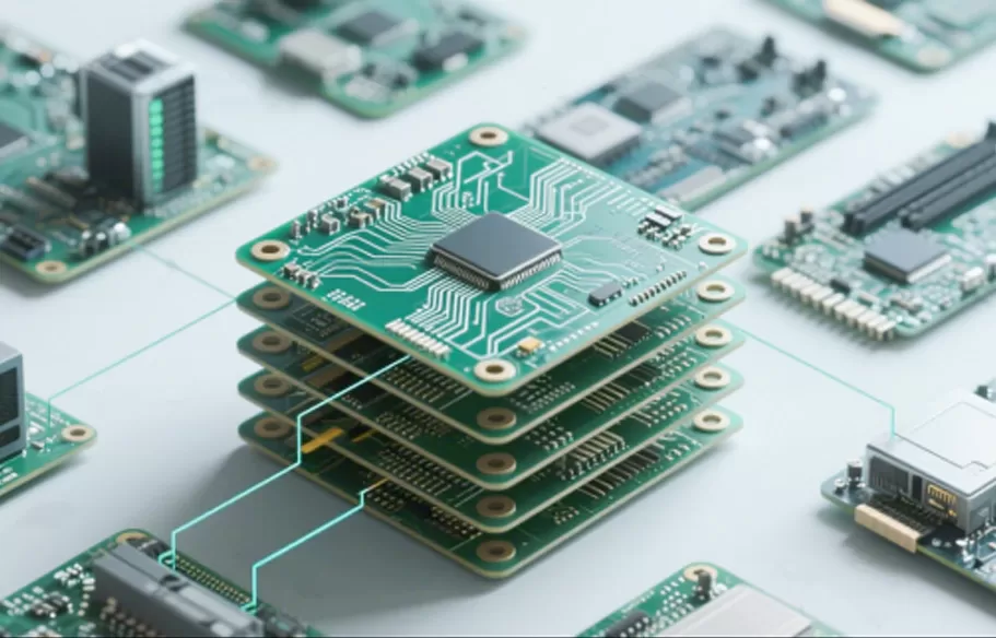
Multilayer PCBs serve as the structural backbone of modern electronic systems. WYD boards are deployed across the following application sectors:
Consumer Electronics and Computing: Smartphones, laptops, tablets, and desktop motherboards rely on 8–16 layer boards for dense component placement, high-speed memory interfaces, and compact form factors. Controlled impedance routing and continuous ground planes maintain signal integrity at multi-GHz data rates.
Telecommunications and 5G Infrastructure: Base station equipment, routers, optical transceivers, and network switches use multilayer boards with hybrid FR-4/Rogers stack-ups for high-frequency signal transmission. Our capability to process mixed-material laminates supports both sub-6 GHz and mmWave applications.
Medical Devices: MRI systems, ultrasound equipment, patient monitors, and portable diagnostic devices demand high-density interconnections and reliable signal quality. Our ISO 13485 certification guarantees medical-grade manufacturing standards for life-critical applications.
Industrial Automation and Robotics: PLC controllers, servo drives, power management systems, and sensor modules require durable boards with stable power planes and reduced signal interference for reliable operation in harsh factory environments.
Aerospace and Defense: Avionics, navigation systems, radar modules, and satellite communication equipment need boards with mechanical strength, thermal resilience, and precise signal routing. High-Tg materials and rigorous reliability testing ensure mission-critical performance under extreme conditions.
Many OEMs judge PCB suppliers only by unit price, ignoring comprehensive support that cuts project risks and shortens R&D cycles. WYD's end-to-end operation system delivers differentiated value for overseas brand and EMS partners across six core areas:
Ready-to-use substrate stock shortens prototype lead time
We stock mainstream high-frequency laminates and full-series FR-4 prepregs on-site, which are all pre-qualified for lamination. Stack-up tuning can begin immediately after DFM review without waiting for raw material procurement.
Global localized tech support eliminates cross-timezone delays
Our local engineering teams based in China's major cities and Italy respond to EU and US clients within their respective working hours, removing communication lag for design revisions and production confirmations.
One-stop design iteration support for prototype optimization
Our technical team assists customers with stack-up adjustment, impedance calibration, and ground plane optimization, and updates production plans rapidly after each Gerber revision to avoid mass-production rework.
Full-process staged inspection to stabilize batch consistency
We set independent quality checkpoints at inner-layer AOI, hole verification, impedance testing, and microsection analysis. Early defect detection lowers scrap rates and guarantees uniform quality across repeat orders.
Unified quality standards for small batches and mass production
Our standardized production line handles five-piece prototypes and thousands of mass-production boards under identical process controls. Clients can scale orders without switching suppliers mid-project.
Strict whole-process IP security for confidential design data
We enforce standardized file management covering Gerber storage, stack-up records, production, and shipment. All proprietary circuit information is fully protected throughout the entire manufacturing cycle.
Multilayer PCB technology has evolved from a specialized manufacturing process into the standard platform for virtually all complex electronic systems. Mastering stack-up design, via architecture, impedance control, and material selection enables engineers to create compact, high-performance products that meet the demands of modern applications.
Whether you need an 8-layer rapid prototype or a 40-layer HDI production run, WeiYuanDa's 20+ years of experience, comprehensive certifications, and global support infrastructure make us a partner you can rely on for consistent quality and on-time delivery.
Q1: What is the maximum number of PCB layers WYD can produce? What are the maximum panel size and minimum drill hole specifications?
A1: WYD has over 20 years of experience manufacturing multi-layer PCBs. Our standard multi-layer boards support up to 24 layers, while high-end HDI high-density interconnect PCBs can reach a maximum of 40 layers. The maximum processing panel size is 1200mm × 600mm. For standard boards, the minimum drill hole diameter is 0.15mm, and high-end HDI boards support microvias as small as 0.10mm by laser drilling, catering to high-density routing demands across communication, industrial control, medical, automotive electronics and other industries.
Q2: What surface finishes do you offer for multi-layer PCBs, and how do I choose the right one?
A2: We provide a full range of mature surface finishes for all multi-layer PCB types: lead-free hot air solder leveling (HASL-LF), electroless nickel immersion gold (ENIG), electroless nickel electroless palladium immersion gold (ENPIG), OSP anti-oxidation, immersion tin, immersion silver and gold finger plating. Our technical engineers offer free material selection recommendations based on your soldering processes, chip bonding requirements and wear resistance needs of edge connectors.
Q3: What is the lead time for PCB prototypes? How about mass production lead time? How fast can I get quotations and DFM reviews?
A3: Simple multi-layer prototypes can be delivered in as fast as 1 working day (only applicable to low-layer boards with standard processes). Formal quotations will be sent within 2 hours after receiving your inquiry. Once we receive your Gerber files, our dedicated engineering team will complete the DFM manufacturability review within 6 hours. Mass production lead times are assessed separately according to layer count, stack-up complexity and special process requirements, and our sales specialists will confirm accurate production schedules with you.