EN
EN
 it
it  fr
fr  de
de  ru
ru  pt
pt  es
es
Get in Touch with WeiYuanDa Now!


The AI industry celebrates transistor counts, FLOPS, and memory bandwidth. But there's a less glamorous problem quietly limiting performance scaling: the physical packaging bottleneck.
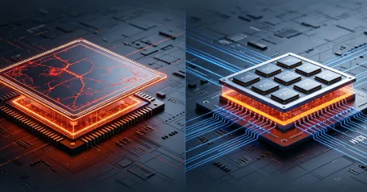
When a modern AI accelerator integrates multiple compute dies, HBM memory stacks, and interconnect bridges into a single package, the PCB underneath must handle extraordinary routing density. Each accelerator package presents an array of I/O pins at ultra-fine pitch—far tighter than conventional PCB manufacturing can accommodate. The system board must accept this high-density interface from multiple chiplets, route those signals without crosstalk or impedance mismatch, and do it all within the mechanical constraints of standard server form factors.
This isn't a silicon problem. It's a PCB problem—and it's why HDI has become as critical to AI hardware as the compute dies themselves.
Industry analysts project the AI server PCB segment to grow at rates that far exceed the broader PCB market average. Every hyperscaler building AI infrastructure is facing the same question: Can our PCB partner actually manufacture what we designed?
Why Monolithic Silicon Hit a Ceiling
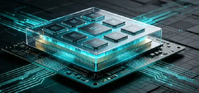
Scaling a single, monolithic die to ever-larger sizes creates compounding problems: reticle limits, yield degradation—a single defect kills an entire giant die—and thermal concentration. Chipmakers solved this by going multi-chiplet.
Modern accelerators now integrate multiple compute chiplets, high-bandwidth memory stacks, and active interposers on a single package. The interposer routes signals at near-semiconductor precision and outputs them to the system PCB through thousands of interconnections. The PCB must accept these high-density interfaces from multiple dies simultaneously, making the board an active participant in the packaging hierarchy rather than a passive carrier.
This transition fundamentally changed what the PCB must deliver. Conventional through-hole technology simply cannot handle the density—the via diameters are too large, the routing channels too scarce, and the layer count required would push board thickness beyond form-factor limits.
The Density Problem Under the Package
A high-end AI accelerator package presents thousands of I/O pins at ultra-fine pitch—densely arrayed across the component footprint. Every pin must be routed out from beneath the package via a dedicated via and trace.
Under a conventional through-hole via approach, a single via consumes space on every layer of the board. With thousands of tightly packed pins, the required routing channels simply don't exist—even with multiple layers, the escape paths cannot accommodate the density.
HDI solves this with two interrelated technologies:
Microvia-in-pad places laser-drilled vias directly under component pads, eliminating the fan-out routing congestion that forces designers to dedicate entire layers just to escape the BGA footprint.
Any-layer interconnect enables vertical signal transitions at any point on the board—not just at board edges—maximizing routing utilization by allowing signals to change layers precisely where needed.
This flexibility is what enables full fan-out from ultra-fine-pitch BGAs. Signals can escape vertically at the pad, route horizontally on the next layer, transition again, and reach the board edge—all without the dead zones that plague through-hole designs. The result: higher pin-count packages fit within the same board footprint, enabling more compute per rack unit.
Materials Evolution for High-Performance AI
The shift toward higher serial data rates in AI systems—PCIe 5.0/6.0 and beyond—demands dielectric materials that can maintain signal integrity over longer trace lengths and through multiple via transitions. Low-loss materials with tightly controlled dielectric constants have become a prerequisite, not an option. However, these materials are fundamentally different from standard FR-4 in their mechanical behavior: they are harder, more brittle, and less forgiving of standard drilling parameters. Manufacturers must recalibrate laser drilling energies, adjust desmear chemistry dwell times, and revalidate copper plating adhesion—each step requiring systematic process development rather than simple parameter adjustments.
Microvia Reliability Under AI Workloads
AI accelerators experience unique stress profiles. Training workloads drive rapid and repeated thermal cycling as the board heats under compute load and cools during idle periods. Each microvia on the board must maintain electrical continuity through thousands of such cycles.
Stacked microvia structures—where multiple microvias are aligned vertically through several layers—are particularly vulnerable to thermal stress. Advanced manufacturers have developed design strategies (staggered vs. stacked configurations) and process refinements (enhanced plating techniques, optimized drilling parameters) that achieve significant reliability improvements over standard processes. These refinements separate qualified AI-grade HDI suppliers from general-purpose PCB fabricators.
Plating Uniformity for Signal Integrity
At ultra-fine trace geometries, copper plating uniformity becomes critical for signal integrity. Inconsistent plating creates trace impedance variations that degrade signal quality and can cause timing skew in differential pairs—a particular concern for the high-speed serial interfaces used in AI systems.
Achieving the tight plating uniformity required for AI-grade boards demands advanced plating systems, precisely calibrated process parameters, and rigorous quality monitoring. This is not standard equipment; it represents a capital and expertise investment that distinguishes AI-capable suppliers from commodity fabricators.
WeiYuanDa Industrial Co., Limited brings over 20 years of PCB manufacturing experience to the AI computing sector—specifically the HDI capability and engineering discipline required to turn multi-die silicon designs into deployable computing infrastructure.
AI-Capable HDI Manufacturing
For AI hardware architects, the PCB isn't a commodity—it's the physical fabric that makes chiplet integration viable. WeiYuanDa's HDI manufacturing platform is purpose-built for this role: sequential lamination processes that sustain the multi-stage buildup AI boards require, plating systems capable of the uniformity needed for sub-50-micron signal integrity, and materials experience that spans the low-loss dielectrics AI designs increasingly specify. This isn't capability available on request—it's capability running in production, validated across thousands of AI accelerator boards.
Engineering Support That Shortens Development Cycles
AI hardware development follows a familiar rhythm: prototype → test → iterate → production. At each stage, board-level issues can derail schedules.
WeiYuanDa provides DFM reviews covering stackup optimization, microvia placement, and lamination stage planning—helping designers avoid manufacturability issues before they reach fabrication. Engineering review is provided quickly, with fast RFQ response for technical queries.
European Local Support
For Nordic and wider European AI hardware teams, WeiYuanDa's Italy-based subsidiary provides direct engineering support, shorter communication loops, and a clearer path from prototype qualification to volume production—without the timezone friction of a purely overseas supply chain.
Beyond HDI
WeiYuanDa manufactures high-frequency, heavy-copper, aluminum, and multilayer boards alongside its HDI portfolio—meaning an AI system that combines high-density compute, high-current power, and RF connectivity can be supported by a single supplier, reducing logistics overhead and quality-handover risk.
The AI computing revolution brings major physical packaging challenges alongside software advances. With multi die, high I/O packages becoming standard, HDI PCB is a decisive factor separating designs that reach volume production from those stalled at qualification.
Your project timelines, field reliability and time to market heavily depend on your PCB partner’s proven expertise in stack up design, sequential lamination, advanced material handling and timely engineering collaboration.
We draw on decades long manufacturing experience, AI optimized HDI capabilities and our European local support network. We deliver reliable manufacturing infrastructure to turn your AI silicon innovations into real world deployments.
To discuss your AI grade HDI PCB requirements or request a quote, visit www.wyd-pcb.com or contact our engineering team at wai.tsang@microstar-pcb.cn.
Q: Why does AI computing require HDI PCB instead of conventional multilayer boards?
A: AI accelerator packages with ultra-fine-pitch BGA and thousands of I/O pins demand microvia-in-pad design and any-layer interconnect that conventional through-hole PCBs cannot physically produce. The routing density required for multi-die package fan-out exceeds what standard manufacturing can achieve.
Q: What are the key manufacturing challenges for AI-grade HDI boards?
A: AI-grade HDI boards demand ultra-high layer counts, extremely dense microvia arrays, multiple sequential lamination stages, and extremely tight plating uniformity tolerances to ensure signal integrity and thermal-cycle reliability. Advanced low-loss materials introduce additional process complexity for drilling and plating.
Q: Can WeiYuanDa support AI hardware development from prototype to production?
A: Yes. WeiYuanDa offers fast prototype turnaround, rapid engineering review, and in-house DFM feedback. Their manufacturing platform supports the layer counts, microvia densities, and material sets required for AI accelerators, scaling from prototype to volume production with ISO 9001, IATF 16949, and UL certifications. European clients receive local support through the WYD Italy office.