EN
EN
 it
it  fr
fr  de
de  ru
ru  pt
pt  es
es
Get in Touch with WeiYuanDa Now!


For industrial buyers sourcing HDI (High-Density Interconnect) printed circuit boards, the critical question is not whether a supplier can produce a prototype — it is whether they can deliver several thousand consecutive production lots with identical electrical and mechanical characteristics. Inconsistent quality in HDI PCB manufacturing leads to costly field failures, production line downtime, and long-term reliability risks. Consequently, the selection of an HDI PCB supplier must be based on verifiable quality management processes rather than promotional claims.
At WYD (WeiYuanDa), our HDI PCB production is governed by a closed-loop quality management system spanning incoming material inspection, in-process monitoring, final electrical testing, and shipment auditing. This document outlines the structural quality framework our team applies across every HDI production batch, providing transparency on how consistent output is achieved. The data referenced throughout corresponds to verified process parameters from our Dongguan production site, which holds ISO 9001, ISO 13485, and IATF 16949 certifications.
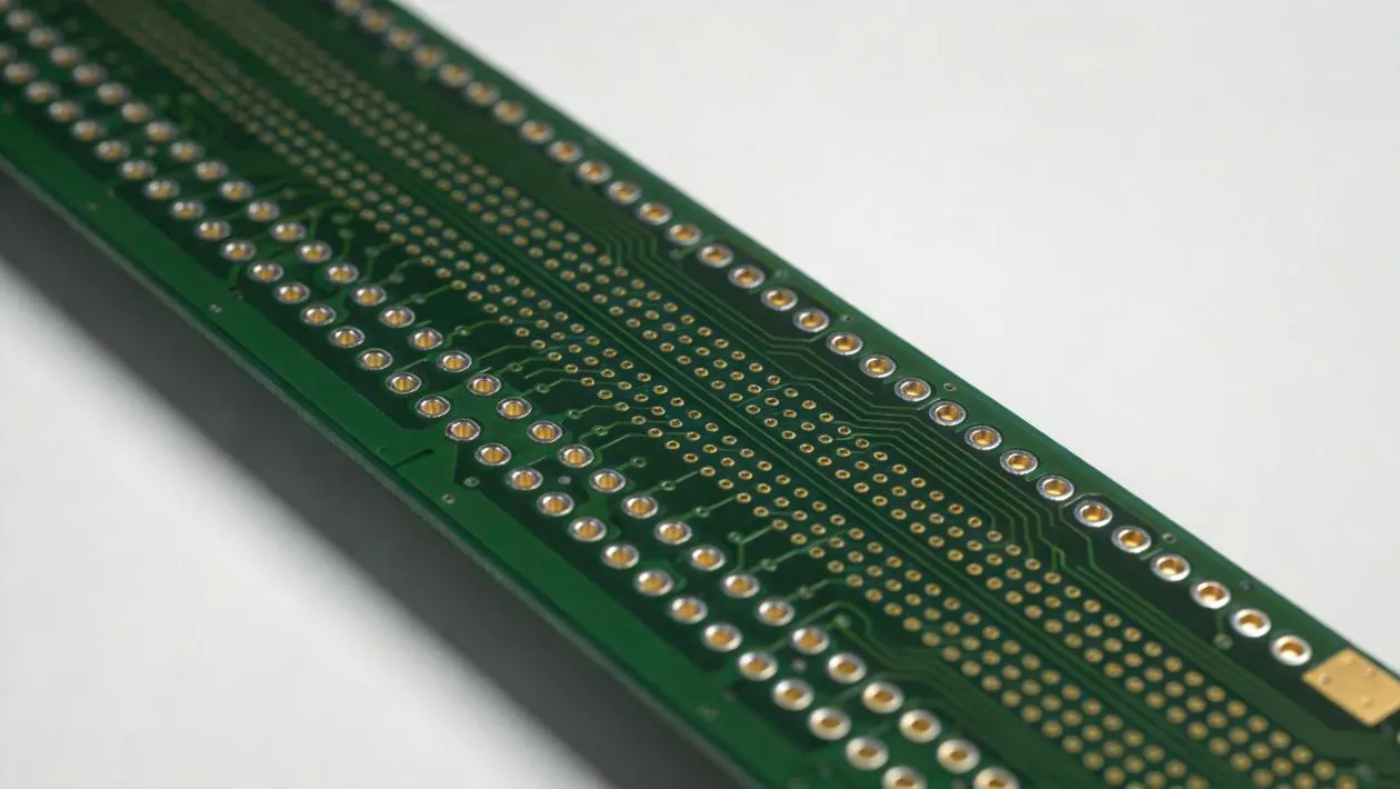
A credible HDI PCB manufacturer operates under internationally recognised management standards that define how processes are documented, audited, and continuously improved. WYD maintains the following active certifications, each addressing a specific dimension of production quality:
Standard | Issuing Body | Relevance for HDI Production |
ISO 9001:2015 | QMS Certification | Foundational quality management system covering process control, document control, and corrective action procedures across all production lines. |
IATF 16949 | Automotive Quality | Automotive-grade quality management with APQP, PPAP, FMEA, and SPC methodologies applied to HDI PCB manufacturing processes. |
ISO 13485 | Medical Devices | Medical device quality management system with enhanced traceability, risk management, and validation requirements for medical HDI applications. |
UL Recognition | UL (USA) | Safety certification for PCB base materials and finished laminates, confirming flammability compliance and dielectric performance. |
ISO 14001:2015 | Environmental Management | Ensures environmentally responsible manufacturing by managing waste, chemical usage, and emissions, which is critical for sustainable HDI production and meeting global green compliance standards. |
HDI PCB manufacturing involves sequential lamination and drilling steps, where errors introduced early become exponentially more expensive to correct later. Our quality control structure is therefore distributed across the production flow rather than concentrated at final inspection. The following six stages define where dimensional, electrical, and material verification takes place:
1. Incoming Material Verification
Every batch of copper-clad laminate, prepreg, and solder mask material is inspected upon receipt against the original material certificate. Our quality team verifies copper foil thickness, dielectric constant, glass transition temperature (Tg), and lot traceability codes. Materials that fail incoming inspection are quarantined and returned to the supplier. For HDI orders requiring FR-4 TG 170 or Rogers 4350 substrates, we additionally confirm material specifications against the customer's Gerber documentation before releasing stock to production.
2. LDI Imaging and Etching Inspection
Laser Direct Imaging (LDI) is used for all inner and outer layer exposure, eliminating the registration variability associated with traditional film-based processes. After etching, an Automated Optical Inspection (AOI) system scans each panel for shorts, opens, and dimensional deviations. For HDI designs with line widths down to 2 mils (approximately 50 micrometres), AOI parameters are calibrated to detect anomalies below 10 micrometres. Any panel exceeding the defined defect rate is routed for manual review and, where economically feasible, rework.
3. Laser Drilling and Plating Validation
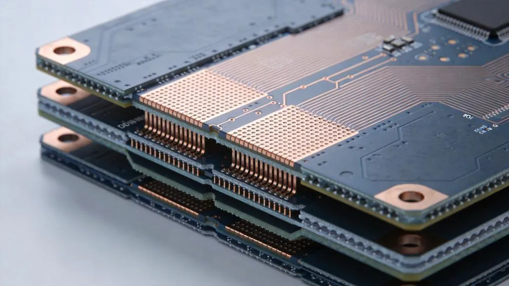
Laser-drilled microvias represent the most critical structural element of an HDI PCB. Our process validates three parameters after each drilling batch: via diameter consistency, via depth uniformity, and copper plating thickness within the via. Cross-sectioning is performed on one coupon per production panel set to verify hole wall quality and plating adhesion. Standard HDI production at WYD maintains a laser via diameter of 0.15 mm with a 1:1 aspect ratio; advanced HDI configurations support 0.2 mm laser vias with a 0.8:1 aspect ratio.
4. Lamination Registration Check
Sequential lamination is the defining process characteristic of multilayer HDI construction. After each lamination cycle, our team verifies layer-to-layer registration using X-ray inspection of tooling holes. Registration deviation must remain below 25 micrometres for standard HDI and below 15 micrometres for advanced HDI configurations. Panels outside these tolerances are rejected before additional processing, preventing downstream waste.
5. Solder Mask and Surface Finish Control
Solder mask application is verified for coverage uniformity, registration accuracy, and minimum solder dam width. For HDI boards with fine-pitch components, solder mask bridge dimensions are measured at 5 mils for standard designs and 3 mils for advanced designs, with 100% AOI inspection of the solder mask layer. Surface finish processes — including HASL, ENIG, OSP, immersion tin, and immersion silver — are each validated by thickness measurement and adhesion testing before the boards proceed to final electrical test.
6. Final Electrical Test and Outgoing Audit
Every HDI PCB produced at WYD undergoes 100% electrical testing using flying probe or dedicated fixture test systems, depending on production volume and test point density. The test program verifies net connectivity and isolation resistance according to the customer's netlist. Following electrical test, a final visual audit is conducted on a sampling basis per ANSI/IPC-A-600 standards. Shipment proceeds only after both electrical test data and visual inspection records are signed off by our quality assurance department.
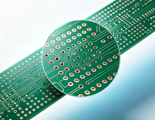
Full traceability is a prerequisite for responsible HDI PCB sourcing. Our production management system assigns a unique lot number to each panel at the beginning of the process and records every subsequent operation, including operator identification, machine parameter settings, inspection results, and timestamp. This lot-level traceability extends backward to incoming material certificates and forward to shipment records, enabling precise root cause analysis in the event of a field quality issue.
Regarding engineering changes, WYD follows a formal change control process. Any modification to material specification, process flow, or tooling requires a written engineering change notice (ECN) with cross-departmental review and customer acknowledgement where the change affects form, fit, or function. Changes are never implemented unilaterally on active production orders without prior written agreement from the customer's technical contact.
Q1. Can WYD supply HDI boards with IPC Class 3 acceptance criteria?
Yes. Standard production follows IPC Class 2 criteria; however, Class 3 inspection criteria are available upon request for high-reliability applications. Customers requiring Class 3 should specify this requirement at the quotation stage so that our process engineers can adjust inspection plans, sampling rates, and test coverage accordingly. Additional documentation, such as first-article inspection reports (FAIR) and process capability studies, can also be provided for qualified programs.
Q2. Is local technical support available for European customers?
Yes. WYD maintains a local sales and technical support office in Formigine (Modena), Italy, staffed with personnel who can assist European customers in Italian and English. Local support includes quotation assistance, technical clarifications, expediting coordination, and on-site consultation where required. European customers also benefit from simplified logistics coordination and closer time-zone communication with our engineering team in Dongguan.
WYD (WeiYuanDa Industrial Co., Limited) is a specialised PCB manufacturer with over 20 years of experience in HDI, multilayer, high-frequency, aluminium, and heavy copper boards. Our Dongguan production site operates 24/7 engineering support, produces approximately 4,000 part numbers per month, and serves customers in more than 50 countries. For inquiries or technical consultation regarding HDI PCB projects, contact our engineering team directly for a response within 2 hours.