EN
EN
 it
it  fr
fr  de
de  ru
ru  pt
pt  es
es
Get in Touch with WeiYuanDa Now!


Quick Answer: A heavy copper PCB supports high current by increasing conductor cross-section and spreading heat, but copper weight alone does not determine capacity. Trace width, layer position, temperature rise, airflow, terminals, vias, copper balance, and the complete thermal path must be evaluated together. |
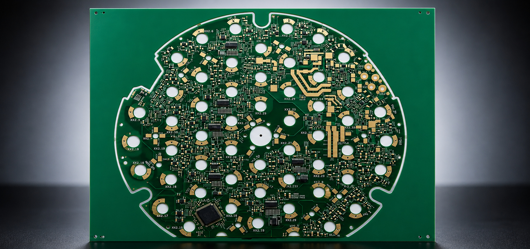
Power supplies, inverters, converters, motor drives, battery systems, industrial controls, and protection equipment often carry currents that exceed the practical range of ordinary signal-board traces.
A well-designed heavy copper PCB for power supply applications can combine control circuits and high-current paths in one assembly, reduce external bus wiring, improve mechanical robustness, and support better thermal distribution. The design must still be validated against real operating and fault conditions.
A heavy copper PCB uses substantially thicker copper than a conventional board, often beginning around 3 oz finished copper in practical purchasing language, although supplier definitions and achievable ranges vary.
The added copper can be used on outer layers, inner layers, selected regions, plated holes, or a combination of these structures. A design may include heavy-current zones beside standard-copper control areas, but mixed-copper constructions require careful etching, plating, lamination, resin fill, and copper-balance review.
The main objective is not simply to make the board heavier. It is to create reliable current paths, acceptable temperature rise, strong interconnections, and manufacturable conductor geometry.
Copper weight increases conductor thickness and therefore cross-sectional area, which can reduce resistance and I²R heating when width and length are unchanged.
Current capacity is not a universal “amps per ounce” value. It depends on trace width, copper thickness, internal or external location, allowable temperature rise, ambient temperature, board material, adjacent copper, airflow, duty cycle, and how heat leaves the assembly. IPC-2152 is the industry reference for determining current-carrying capacity in printed-board design.
A high current PCB design should be based on a defined temperature-rise limit and verified with the actual stack-up. Narrow transitions, thermal relief spokes, connector pads, fuse links, via arrays, and neck-downs can become the hottest points even when the main conductor is wide.
The best conductor is the one that meets electrical, thermal, spacing, and manufacturing requirements with sufficient margin.
Increasing trace width is often more cost-effective than increasing copper weight when board area is available. Thick copper becomes valuable when space is limited, mechanical strength is needed, plated-hole current must increase, or the design benefits from integrated bus structures.
Use simulation or an IPC-based design tool for the first estimate, then review the result with the fabricator. Prototype thermal testing should include continuous load, peak load, fault or surge conditions where applicable, and the highest expected ambient temperature.
Design Factor | Effect on Performance | Review Question |
Finished copper thickness | Changes conductor cross-section, etching difficulty and plated-feature geometry | Is the specified value base copper or finished copper? |
Trace width and length | Directly affects resistance and voltage drop | Where are the narrowest high-current sections? |
Internal vs external layer | Internal conductors usually dissipate heat less effectively | Can the main power path use external copper or larger planes? |
Via and plated-hole structure | Transfers current between layers and may create bottlenecks | Are hole size, plating thickness and via count adequate? |
Allowable temperature rise | Defines the thermal design target | What maximum conductor and component temperature is acceptable? |
Terminal and connector interface | Contact resistance can dominate local heating | Are pad size, plating, fastener pressure and current rating controlled? |
Heavy copper spreads and conducts heat, but the board still needs a defined path to the surrounding air, chassis, cold plate, or heat sink.
Power semiconductors, rectifiers, shunts, transformers, inductors, and connectors may create concentrated hot spots. Use broad copper areas, short current loops, appropriate thermal vias, direct metal contact where allowed, and component placement that prevents heat-sensitive control circuits from sitting beside the hottest devices.
The WYD heavy copper PCB page describes manufacturing options for thick-copper structures, while the energy power supply PCB solution page connects those capabilities with inverter, converter, rectifier, and high-current application requirements.
High current and high voltage are separate design problems: thick copper may reduce conductor resistance, but it does not replace adequate electrical spacing and insulation design.
Working voltage, pollution degree, material group, altitude, transient category, coating, slots, and applicable product standards can affect creepage and clearance. Thick-copper etching also changes conductor sidewall geometry, so the fabrication capability and final spacing after processing must be considered.
Where power and control circuits share a board, define isolation boundaries clearly and avoid routing low-level sensing traces through noisy switching-current paths. Kelvin connections for current shunts and controlled return paths can improve measurement accuracy.
Heavy copper designs need early DFM because plating distribution, etching compensation, resin filling, lamination pressure, hole-wall reliability, solder mask coverage, and board flatness are more demanding than on standard boards.
Provide finished copper requirements by layer, stack-up, minimum conductor width and spacing, via current assumptions, plated-hole dimensions, tolerance, surface finish, panel constraints, and acceptance criteria. Electrical testing should be combined with cross-section review, AOI, dimensional inspection, and any required thermal or current-load validation.
WYD PCB capability information can support a discussion of inspection and process control before tooling. For quotation, include Gerber or ODB++, fabrication notes, current map, voltage limits, expected temperature rise, and production volume.
Many buyers use 3 oz or more as a practical threshold, but definitions vary. Always state the required finished copper thickness by layer.
No. Current capacity also depends on width, layer location, temperature rise, airflow, surrounding copper, length, and the thermal path.
Yes, mixed-function boards are possible, but copper balance, spacing, etching, lamination, noise control, and DFM become more complex.
Designers may use plated holes, via arrays, copper-filled structures, press-fit connections, terminals, or embedded bus features. The chosen method must be checked for current density and reliability.
Provide stack-up, finished copper by layer, current and voltage maps, temperature-rise limit, minimum geometry, hole requirements, surface finish, mechanical drawing, and test criteria.
Test voltage drop and temperature at continuous and peak load under worst-case ambient and cooling conditions, while monitoring terminals, vias, neck-downs, semiconductors, and magnetic components.