EN
EN
 it
it  fr
fr  de
de  ru
ru  pt
pt  es
es
Get in Touch with WeiYuanDa Now!


Quick Answer: A single-sided PCB has one conductive copper layer and is best suited to circuits with low routing density, stable product volumes, straightforward electrical requirements, and strong cost pressure. It is often the most efficient option for simple power, lighting, control, interface, and consumer-electronics functions. |
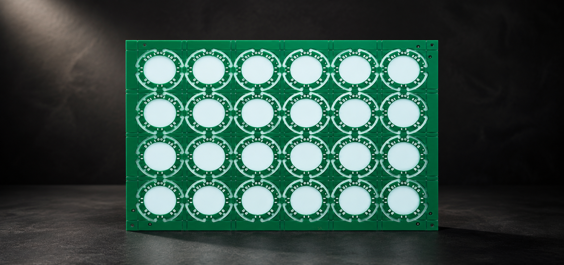
Single-layer boards remain widely used because not every product benefits from additional layers. A simple circuit built on a well-designed one-layer board can be easier to inspect, less expensive to fabricate, and highly repeatable in volume production.
This sourcing guide explains when to choose a one-layer construction, when to move to a double-sided or multilayer board, and what information a single sided PCB manufacturer needs to quote accurately.
A single-sided PCB uses one copper circuit layer on one side of the insulating substrate, with component mounting and interconnection arranged to suit that one-layer routing structure.
Through-hole components are often mounted on the opposite side from the copper and soldered through drilled holes, while surface-mount components may be assembled directly on the copper side. Jumpers, zero-ohm resistors, wire links, or component leads can bridge unavoidable crossings.
Common substrates include FR-4, CEM-1, CEM-3, paper phenolic grades, and metal-core materials depending on electrical, thermal, mechanical, flammability, and cost requirements.
A single-layer construction is most effective when the schematic is simple enough to route without excessive jumpers, the operating frequency is modest, and component density does not require internal planes or complex interconnection.
Typical uses include LED lighting modules, small power supplies, relay boards, appliance controls, chargers, sensor interfaces, toys, remote controls, display boards, simple automotive lighting, and industrial subassemblies.
WYD’s single layer PCB page provides a direct route to discuss materials, dimensions, copper, surface finish, prototype quantity, and production requirements with a single layer PCB manufacturer.
A higher-layer-count board becomes more practical when routing congestion, signal return paths, EMI control, power distribution, connector density, or mechanical size cannot be solved cleanly on one copper layer.
If a single-layer layout requires many wire jumpers, long loop areas, narrow power traces, or awkward component placement, a double-sided board may reduce assembly labor and electrical risk even if the bare-board price is higher. Multilayer construction is generally preferred for dense digital systems, controlled impedance, high-speed interfaces, BGA escape routing, and complex power-ground structures.
The correct decision should consider total assembled cost, quality risk, test time, enclosure size, and production yield rather than only the PCB unit price.
Board Type | Best For | Advantages | Limitations |
Single-sided PCB | Simple, cost-sensitive, stable high-volume circuits | Lowest routing complexity, easy inspection, efficient fabrication | One copper layer, limited routing and plane options |
Double-sided PCB | Moderate component density and routing | More compact layout, plated interconnections, fewer jumpers | Higher fabrication complexity and cost |
Multilayer PCB | Dense, high-speed, high-function electronics | Power/ground planes, controlled returns, high routing density | More design control, lamination steps and testing |
Single-layer aluminum PCB | LED and power circuits needing metal-base cooling | Simple routing plus strong heat spreading | Limited routing density and specialized thermal/mechanical design |
The substrate controls electrical insulation, heat resistance, mechanical stiffness, drilling or punching behavior, flammability, moisture performance, dimensional stability, and cost.
FR-4 is broadly used when stronger mechanical and thermal performance is needed. CEM-3 can be attractive for selected single- and double-sided applications because specific grades offer good processability and electrical performance. Paper-based laminates may be considered for very cost-sensitive consumer products when the product requirements allow them.
For high heat density, a conventional laminate may not be sufficient. An aluminum PCB can provide a more direct thermal path for LEDs and power components, but it requires a separate thermal and mechanical review.
A manufacturable one-layer design uses simple routing, adequate conductor width and spacing, clear component orientation, robust annular rings, and a panel strategy suited to the expected volume.
Keep high-current paths short and wide, separate high-voltage areas, avoid unnecessary acute angles, and place connectors and heavy components where mechanical load can be supported. Confirm finished hole sizes after plating, lead diameters, soldering method, component insertion direction, and whether the assembly will use wave soldering, selective soldering, hand soldering, or SMT reflow.
For punched CEM or paper-based boards, hole and outline tolerances may differ from routed FR-4. For V-scoring, routing, or stamp holes, the panel and depaneling method should be defined before release.
A capable supplier should confirm material availability, copper and thickness tolerance, minimum geometry, drilling or punching method, surface finish, solder mask, legend, panelization, electrical test, inspection, and lead time.
Request a DFM review for any design with high current, high voltage, unusual outline, heavy components, tight tolerances, or a nonstandard laminate. WYD PCB capability information can help procurement teams understand available manufacturing and inspection resources.
For repeat production, agree on material brand or approved equivalents, controlled characteristics, change-notification rules, golden sample, test data, packaging, shelf life, and traceability.
A complete data package reduces clarification time and prevents a low-cost board from becoming an expensive assembly problem.
· Gerber or ODB++, drill data, board drawing and netlist if available.
· Material grade, finished thickness, copper weight and flammability requirement.
· Minimum conductor width and spacing, hole tolerances and special slots or cutouts.
· Surface finish, solder mask, legend, carbon ink, peelable mask or other special processes.
· Panel size, breakaway method, fiducials, tooling holes and assembly direction.
· Prototype quantity, forecast volume, target lead time and packaging requirement.
· Electrical test, dimensional report, first article, certificate or traceability requirements.
The terms are generally used for the same construction: one conductive copper layer on the substrate.
No. They are a valid engineering choice for simple functions and can deliver excellent reliability when the design, material, process, and assembly are appropriate.
Yes. SMT parts can be placed on the copper side, and mixed SMT/through-hole assemblies are also common.
When a one-layer design needs many jumpers, extra assembly labor, larger board area, or compromises in current path and EMI performance, a double-sided board may reduce total cost.
Compare material control, finished tolerances, process capability, electrical test, inspection, change control, lead time, communication, and support for prototype-to-volume transfer.
Yes. The substrate can be selected according to cost, thermal, electrical, mechanical, flammability, and processing requirements.