EN
EN
 it
it  fr
fr  de
de  ru
ru  pt
pt  es
es
Get in Touch with WeiYuanDa Now!


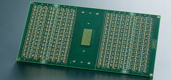
As wireless communication, automotive millimeter radar, aerospace RF modules, and industrial IoT push operating frequencies above 500 MHz up to 77 GHz, ordinary FR-4 PCBs fail to sustain stable signal transmission. Tiny shifts in dielectric performance, copper smoothness and line precision trigger severe insertion loss, signal reflection, and EMI interference, ruining overall equipment performance. To solve these RF bottlenecks, engineers rely on high-frequency PCBs built with low-loss laminates, and WeiYuanDa (WYD) stands as a reliable full-cycle manufacturer specializing in customized high-frequency PCB prototyping and mass production for global OEMs.
This in-depth engineering manual compiled by our internal RF engineering team, covers core high-frequency PCB theories, unique manufacturing pain points, mainstream RF substrate solutions, industry-wide application cases, and the full set of proprietary production strengths only available at WYD. We integrate our 20+ years of RF board fabrication experience to explain how our precise process control solves common GHz signal integrity issues for clients across over 50 countries.
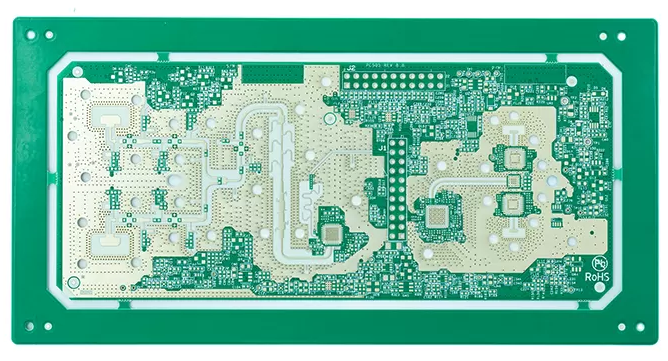
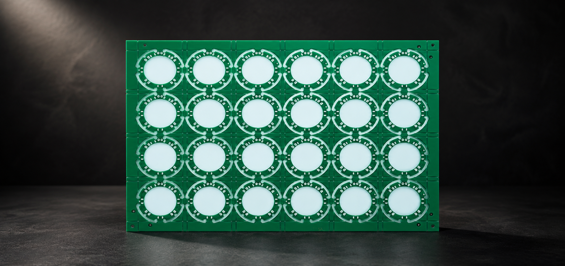
All design and manufacturing rules for high-frequency circuits adopted by WYD are tailored to eliminate high-frequency signal attenuation, with every process standard strictly calibrated for 500 MHz–77 GHz signals.
Signal Integrity at the Core
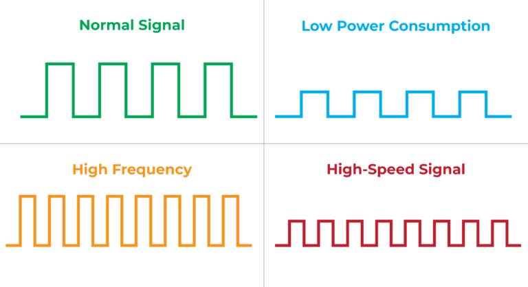
At GHz frequencies, the wavelength of electromagnetic signals shrinks dramatically. A 10 GHz signal has a wavelength of only 30 mm in free space — meaning even small PCB trace discontinuities can act as antennas, radiating energy and causing reflections. High frequency PCBs address this by using substrates with tightly controlled dielectric constant (Dk 2.0–3.6) and extremely low dissipation factor (Df 0.001–0.003), ensuring signals propagate with minimal attenuation and phase distortion.
Precision Geometry Requirements
Unlike standard digital boards where trace widths of 5–8 mils are acceptable, high frequency designs demand line widths and spacings accurate to the micrometer level. Controlled impedance traces — whether microstrip or stripline configurations — must maintain consistent geometry across the entire signal path. Surface treatments such as ENIG (Electroless Nickel Immersion Gold) or immersion silver are preferred for their smooth, uniform copper interfaces that minimize conductor loss at high frequencies.
Thermal and Environmental Stability
RF laminates must maintain stable electrical performance across temperature extremes. Materials like Rogers RO4350B offer thermal conductivity of 0.3–0.8 W/m·K combined with low thermal expansion coefficients, preventing impedance drift during thermal cycling. This stability is critical for applications like 5G base stations and military radar that operate continuously in harsh outdoor environments.
Choosing the right dielectric material is the single most impactful decision in high frequency PCB design. The material directly determines signal loss, impedance consistency, and long-term reliability. At WYD, we stock and process the four most widely specified RF laminate families, allowing engineers to balance performance, manufacturability, and cost.
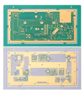
Rogers Laminates (RO4350B, RO3003, RO3010): The industry benchmark for advanced RF and microwave designs. Rogers materials deliver stable Dk values from 3.0 to 10.2 with ultra-low Df down to 0.0013, supporting broadband performance up to 77 GHz. They are the go-to choice for 5G base station antenna feed networks, phased array systems, and RF power amplifiers where signal integrity is non-negotiable.
Taconic Laminates (TLX, RF-35): Known for superior thermal stability and minimal moisture absorption. TLX provides low insertion loss and excellent dimensional stability for multi-GHz RF switches and high-speed transmission lines. RF-35 offers a cost-effective alternative compatible with standard PCB manufacturing processes, making it ideal for both prototyping and full-scale production.
Arlon 85N: Engineered for extreme environments. With Tg of 250°C, thermal conductivity of 0.20 W/m·K, and strong peel strength, Arlon 85N withstands high-power radar transmitters and aerospace RF modules where both electrical precision and mechanical durability are essential.
Isola IS620 (E-Glass Reinforced): A practical mid-range option. Stable electrical properties up to 10 GHz at a lower cost point than PTFE systems. Suitable for consumer electronics and telecom products operating below 5 GHz where full high-frequency performance is not required.
Material | Key Properties | Frequency Range | Typical Applications |
Rogers (RO4350B, RO3003) | Stable Dk (3.0–10.2), ultra-low Df (0.0013) | Up to 77 GHz | 5G base stations, antenna feed networks, phased arrays |
Taconic (TLX, RF-35) | Low insertion loss, good thermal stability | Multi-GHz | RF switches, microwave circuits, telecom equipment |
Arlon 85N | Tg 250°C, thermal conductivity 0.20 W/m·K | High-power GHz-class | Aerospace RF modules, defense radar |
Isola IS620 | E-glass reinforced, stable up to 10 GHz | < 5–10 GHz | Consumer electronics, telecom devices |
WYD also supports hybrid stack-up designs where critical high-frequency signal layers use Rogers or PTFE while non-critical layers use standard FR-4 — delivering high-frequency performance without unnecessary material cost on every layer.
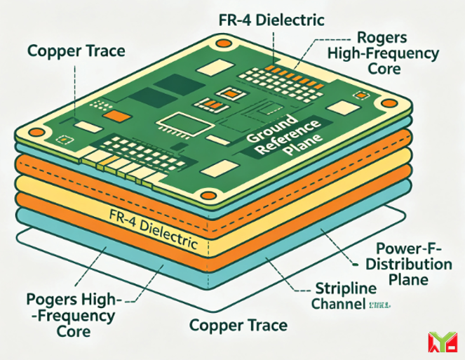
Building a high frequency PCB is not simply a matter of substituting one laminate for another. The manufacturing process itself introduces variables that can make or break RF performance. Understanding these challenges helps engineers specify realistic tolerances and choose a manufacturer with the right process controls.
Copper Foil Surface Roughness
At GHz frequencies, current flows primarily on the surface of copper traces due to the skin effect. A rougher copper surface effectively increases the signal path length, raising insertion loss. High frequency PCB manufacturers must use smooth rolled or reverse-treated copper foils — typically with RMS roughness below 1 μm — to minimize this effect.
Solder Mask Dielectric Impact
Standard solder masks have relatively high dissipation factors that add dielectric loss when covering RF traces. In high frequency designs, selective solder mask application or solder mask defined (SMD) pads require careful layout to avoid introducing unintended impedance variations. Some critical designs use solder mask windowing to expose RF traces entirely.
Via Stub Reflections
In multi-layer high frequency PCBs, unplated via stubs above the signal layer act as resonant antenna elements, causing signal reflections at specific frequencies. Back drilling — a precision process that removes the unused stub portion — is essential for maintaining signal integrity in boards operating above 5 GHz. WYD offers controlled-depth back drilling as a standard capability for high frequency multilayer boards.
Dimensional Stability and Layer Registration
RF laminates have different thermal expansion coefficients than standard FR-4. During lamination and subsequent thermal processing, mismatched expansion can shift trace geometry or cause layer misregistration, both of which degrade impedance control. Our manufacturing process uses precision alignment systems and controlled thermal profiles to maintain ±0.05mm registration accuracy even on 12-layer Rogers stack-ups.
High frequency PCBs serve as the invisible backbone of modern communication and sensing infrastructure. Our boards are shipped to OEMs and R&D companies across 50+ countries, with key application areas including:
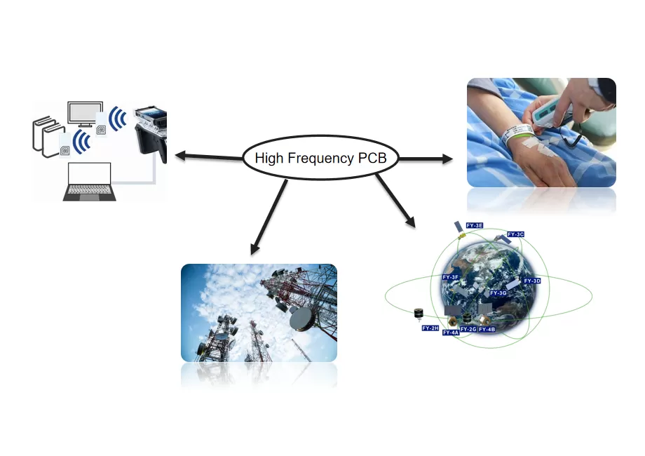
5G Telecommunications: Base station antenna modules, power amplifiers, and RF transceiver units rely on Rogers-based high frequency boards for consistent signal transmission at mmWave frequencies. Our boards are deployed in commercial 5G infrastructure across Europe and Asia.
Aerospace and Defense: Satellite communication transceivers, navigation system RF front-ends, and military radar modules need boards that perform reliably across extreme temperature ranges. Arlon 85N-based boards from WYD meet the stringent reliability standards of these applications.
Medical Imaging Equipment: MRI systems and ultrasound devices use high frequency PCBs for precise signal processing in RF coils and transducer arrays. Our ISO 13485 certification ensures medical-grade quality for these life-critical applications.
Industrial IoT and RFID: RF identification readers, microwave sensors, and industrial wireless modules benefit from cost-effective high frequency boards using Isola IS620 or Taconic RF-35, balancing performance with production economics.
WeiYuanDa (WYD) is not just a fabricator — we are a high frequency PCB manufacturing partner that works closely with design engineers from prototype through mass production. Here is what sets us apart:
20+ Years of RF Manufacturing Experience: Founded in Hong Kong in 2005 with production facilities in Dongguan, WYD has accumulated over two decades of expertise in complex multilayer and high frequency PCB fabrication. 65% of our 250+ team members bring 10+ years of skilled PCB manufacturing experience.
Large-Scale Material Inventory: We maintain in-house stock of Rogers, Taconic, Arlon, and Isola RF laminates — eliminating lead time delays associated with material procurement. This means faster prototype turnaround and more consistent supply chain for mass production orders.
Full-Certification Quality System: Our factory holds ISO 9001, ISO 14001, ISO 13485, IATF 16949, and UL certifications for the US and Canada markets. We are also an IPC member with CIS certifications, reflecting our commitment to international quality standards.
Advanced Engineering Capabilities: Our 24+ engineer team provides DFM review within 6 hours, with expertise in controlled depth drilling, back drilling, precision milling, and hybrid FR-4/Rogers stack-up design. RFQ responses are provided within 2 hours, and prototype delivery starts from as fast as 1 working day.
Global Service Network: With local sales and technical support offices in Beijing, Chengdu, Xi'an, Shanghai, Shenzhen, and Italy, WYD delivers localized support for clients worldwide. We currently serve customers in over 50 countries, with a strong focus on European and North American markets.
End-to-End Production Under One Roof: From Gerber file processing and stack-up optimization through fabrication, impedance testing, and final inspection — all processes are managed in-house. This vertical integration ensures consistency, faster iteration, and fewer handoff errors compared to outsourced manufacturing chains.
High frequency PCB design demands more than just theoretical knowledge — it requires a manufacturing partner who understands the intersection of material science, precision fabrication, and real-world RF performance. From Rogers RO4350B antenna modules to 12-layer hybrid stack-ups for automotive radar, WeiYuanDa delivers the quality, speed, and engineering support that GHz-class projects demand.
Whether you need a quick-turn prototype or mass production of complex RF boards, WYD's 20+ years of experience, comprehensive certifications, and global support network make us a partner you can count on.
Q1: When do I need high-frequency PCBs instead of standard FR-4 boards?
A1: Circuits working above 500 MHz require low-loss RF laminates. FR-4 has high dielectric loss at GHz frequencies and cannot support 77GHz radar or mmWave 5G devices.
Q2: What is the advantage of hybrid stack-up PCB?
A2: Hybrid designs use high-frequency materials for critical RF layers and FR-4 for power/ground layers, balancing RF performance and overall material cost.
Q3: What precision tolerances can WYD achieve for RF boards?
A3: WYD guarantees ±0.05mm layer alignment, 2 mil minimum line width/spacing for HDI, and copper roughness below 1μm to stabilize impedance.