EN
EN
 it
it  fr
fr  de
de  ru
ru  pt
pt  es
es
Get in Touch with WeiYuanDa Now!


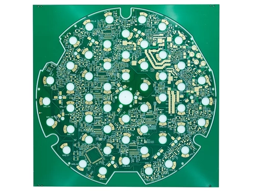
High-power electronic products such as solar inverters, EV motor drive boards, industrial servo controllers and server power modules always face two core design pain points: excessive temperature rise of power chips and obvious voltage drop caused by large current. Ordinary PCBs with 1/3oz, 0.5oz, and 1–2oz thin copper cannot bear long-term heavy current load, and local hot spots will lead to solder joint cracking, device aging and frequent after-sales failures. Heavy copper PCB adopts ultra-thick copper conductive layers from up 10oz or above, which fundamentally solves the dual problems of high current transmission and heat dissipation, and becomes the core carrier of modern high-density power equipment.
This WYD handbook systematically sorts out the structural characteristics, core competitive strengths, design specification standards, mainstream application fields of heavy copper PCB, and teaches you how to screen qualified manufacturers to avoid thermal overload and circuit burnout risks in prototype trial production and mass production stages.
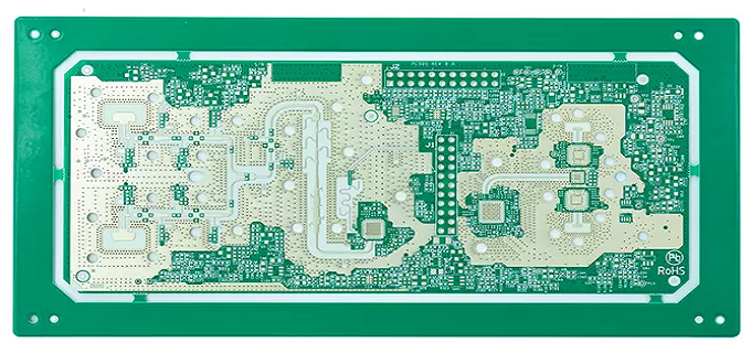
Different from conventional PCB’s thin copper etching process, heavy copper PCB relies on special thick copper electroplating and precision etching technology, with multi-layer composite structure optimized for high power and heat conduction. Its four core structural modules are as follows:
Ultra-Thick Copper Conductive Layer
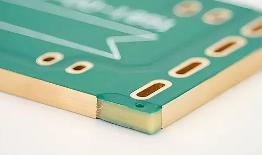
This is the core marking of heavy copper boards. The industry’s standard heavy copper specification starts at 3oz (about 105μm), and the maximum customizable thickness reaches 15oz. The thicker copper cross-section greatly reduces circuit resistance, and large-area copper planes can quickly spread heat generated by MOSFET, IGBT and other power devices. Both outer wiring layers and inner power/ground layers support customized thick copper stacking.
Base Substrate Carrier
FR-4 high Tg substrate is the mainstream matching material, with halogen-free substrate, aluminum metal core substrate and high-frequency special substrate as optional schemes for special working conditions. High Tg substrate can resist thermal deformation under alternating cold and hot cycles, such as Tg 170 to Tg 280 effectively preventing board warpage, interlayer separation and copper layer shedding caused by thick copper thermal expansion.
Insulation Prepreg Dielectric Layer
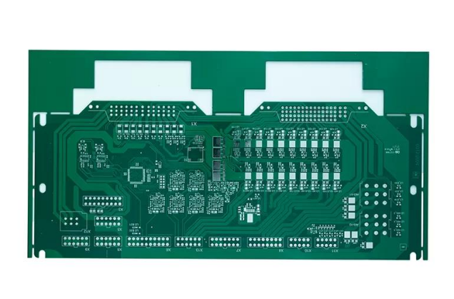
High bonding strength prepreg separates each thick copper circuit layer, which can maintain stable electrical insulation while providing auxiliary vertical heat conduction channels between layers, balancing insulation safety and heat dissipation efficiency.
Multi-Type Surface Treatment Layer
Optional surface processes include ENIG, OSP, HASL and immersion tin. ENIG surface finish is widely used in automotive, medical and industrial high-reliability equipment, which improves oxidation resistance and welding stability of pads; OSP is more suitable for mass-produced cost-sensitive power products.
The product structure supports single-sided, double-sided and multi-layer stacked schemes. Multi-layer heavy copper boards are preferred for compact high-power equipment that needs dense signal wiring and large current transmission at the same time.
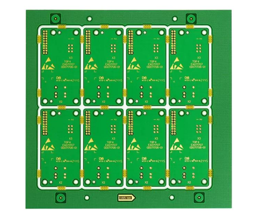
The thick copper structural design brings comprehensive performance improvement to high-power hardware, and its advantages cannot be replaced by ordinary thin copper circuit boards in high-temperature, high-current and vibration harsh environments:
Powerful Large-Current Bearing Capacity
The increase of copper thickness directly expands the conductive cross-sectional area, greatly reduces circuit impedance. Thick copper traces can stably pass dozens of amperes of continuous working current and resist instantaneous large surge current, effectively restrain voltage drop of power loops and reduce power loss. For EV BMS and industrial inverter circuits, it completely eliminates the hidden danger of circuit burnout caused by overload thin traces.
Built-In High-Efficiency Heat Dissipation System
Copper has ultra-high thermal conductivity up to 401 W/m·K. The large-area thick copper plane is equivalent to an integrated heat sink, which quickly diverges the heat of power components to the whole board. Compared with conventional FR4 thin copper boards, the junction temperature of chips can be reduced by 15–20°C, slowing down the aging speed of electronic devices and extending the overall service life of equipment. It also reduces the number of external heat sinks, simplifies the mechanical assembly structure of products and lowers BOM cost.
Strong Anti-Vibration & Thermal Cycle Reliability
Thick copper foil forms firmer bonding with substrate prepreg. PTH holes and connector pads have stronger mechanical bearing capacity, and will not crack under long-term vibration and thermal shock alternating tests. After hundreds of high-low temperature cycle experiments, the circuit remains intact without delamination or trace fracture, fully meeting the strict reliability standards of automobile and aerospace industries.
Realize Miniaturization of High-Power Equipment
Relying on excellent current-carrying and heat dissipation performance integrated on the board, designers can appropriately reduce the overall size of the circuit board without sacrificing power output. Thick copper planes can replace independent busbars and auxiliary heat-conducting accessories, simplify product assembly procedures and shorten production cycle.
Flexible Matching With Composite Process Technology
Heavy copper technology can be combined with aluminum substrate, metal core, blind buried vias and other processes to form composite heat dissipation boards, which is suitable for ultra-high power LED, compact power supply and other scenarios with extreme heat dissipation requirements.
Low-power signal control boards do not need heavy copper technology, but for all high-current and high-heat electronic equipment, heavy copper PCB is an indispensable core carrier:
New Energy & Electric Vehicle Electronics
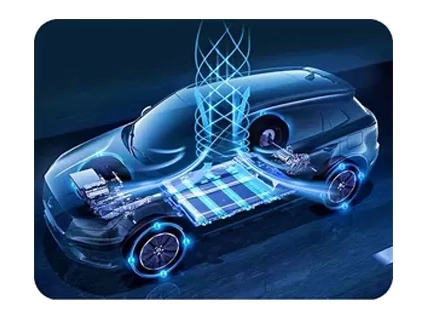
On-board chargers, motor drive control boards, BMS battery management systems and vehicle lamp power modules work in environments with severe temperature changes and continuous vibration. Heavy copper PCB stabilizes power transmission and controls temperature rise, fully complying with IATF 16949 automobile industrial quality certification standards.
Industrial Automation & High-Power Power Equipment
Industrial inverters, servo drives, welding power supplies, UPS standby power supplies and high-power AC-DC converters rely on heavy copper boards to bear continuous heavy current, reduce heat accumulation of circuits, and ensure stable long-time operation of factory equipment.
5G Communication & AI Computing Hardware
5G base station power supply units and AI server power modules are installed in narrow cabinets with poor ventilation. Heavy copper PCB optimizes the overall thermal management, keeping power chips operating within safe temperature range under 24-hour uninterrupted working state.
With over 20 years of experience in metal core and heavy copper PCB manufacturing, WYD PCB specializes in precision custom boards for high-power thermal management devices, boasting stronger technical capabilities than regular PCB manufacturers.
We run a full-process closed-loop quality control system with AOI testers, microsection analyzers and thermal shock machines to inspect copper adhesion, dielectric insulation and circuit integrity for every batch. Our factory holds full certifications including ISO 9001, ISO 14001, ISO 13485, IATF 16949 and UL certificates for North America and Canada.
Our engineering team delivers full-cycle one-stop support from DFM review and fast prototyping to mass production. We serve global OEMs across automotive electronics, new energy, industrial automation and telecom servers, balancing precision, thermal performance and cost to supply reliable PCB solutions for high-power product development.
With the continuous improvement of electronic power density and the continuous miniaturization of product shell space, heavy copper PCB has changed from a small-batch customized accessory to a standard design scheme for all high-power electronic equipment. Mastering its internal stacking structure, copper thickness selection and standardized design specifications can help engineers effectively eliminate hidden dangers such as thermal overload and high-current circuit burnout.
When selecting heavy copper PCB manufacturers, it is suggested to take the factory’s mature thick copper process capability, complete reliability testing system and timely engineering technical response as the core evaluation standards, instead of only focusing on the unit price of finished boards. A professional manufacturing partner can greatly reduce design iteration times, avoid prototype scrap loss, and accelerate the speed of new high-power products to market.
Q1: Is the thicker copper layer of heavy copper PCB always better?
Not completely. Although thicker copper improves current-carrying capacity and heat spreading performance, excessively thick copper will increase manufacturing difficulty and production cost, and limit the minimum line width of fine signal wiring. The copper weight should be determined comprehensively according to the actual working current, layout wiring density and thermal budget target of the product.
Q2: What design documents need to be provided for heavy copper PCB quotation?
You need to prepare Gerber or ODB++ design files, board manufacturing mechanical drawings, detailed stacking specifications (copper thickness, substrate type, total layers), working voltage demand, surface treatment selection, order quantity and delivery cycle requirements.
Q3: Can heavy copper PCB be combined with aluminum metal substrate technology?
Yes. Aluminum-based heavy copper PCB integrates thick copper circuit and aluminum heat dissipation substrate, and has ultra-high comprehensive thermal conductivity, which is widely used in high-power LED lighting and compact power modules with strict heat dissipation requirements.
Q4: Is WYD PCB with heavy copper UL certification?
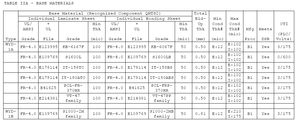
Yes. WYD had been approved with UL for heavy copper up to inner layer with 5oz and outer layer with 6oz. The CCL we being approved for heavy copper PCBs are KB6167, S1600L, IT158TC, IT180TC,PCL-FR-370HR,VT-47 Family & S1000-2M Family.
About the Author
This technical guide is compiled by the professional R&D engineering team of WYD PCB, a leading Chinese manufacturer integrating heavy copper PCB and aluminum substrate PCB production, serving global electronic OEM customers for more than two decades. For technical consultation or instant quotation, you can browse wyd-pcb.com to submit your demand.