EN
EN
 it
it  fr
fr  de
de  ru
ru  pt
pt  es
es
Get in Touch with WeiYuanDa Now!


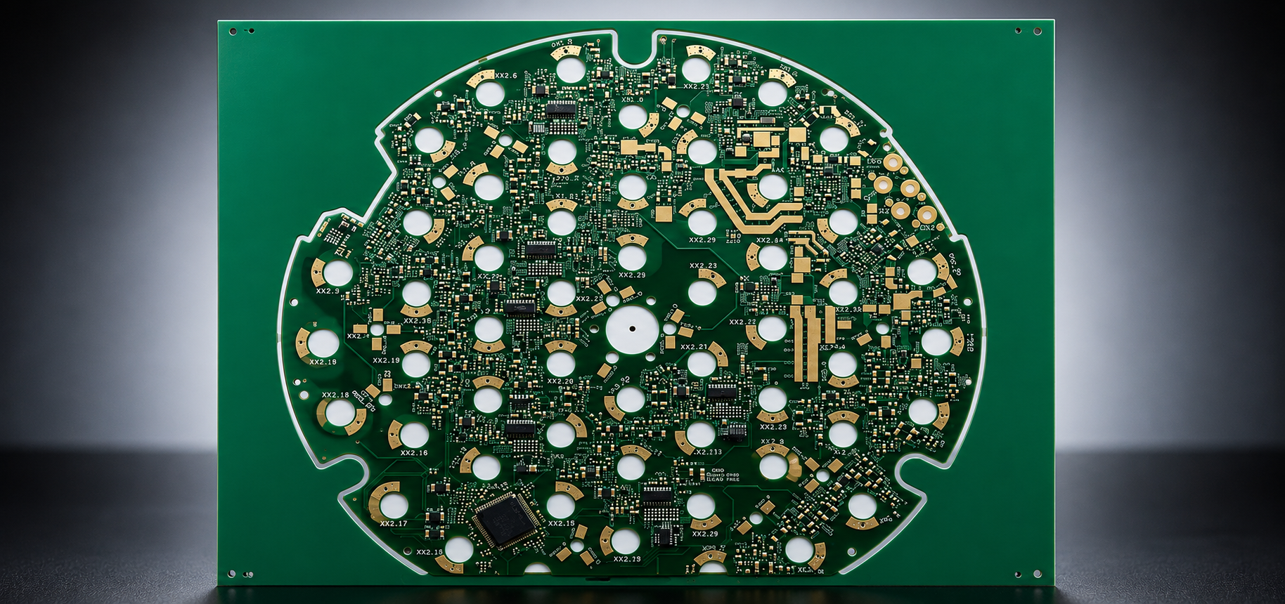
Wearable devices are shrinking. Health monitors, AR glasses, smart rings, continuous glucose sensors—they all demand more functionality packed into smaller enclosures with tighter ergonomic constraints. The circuit board at the heart of these devices faces a fundamental contradiction: component density keeps rising while available space keeps falling.
This is where HDI PCB technology becomes non-negotiable rather than optional.

Modern wearables integrate sensors, wireless modules, power management, and application processors into form factors measured in centimeters or millimeters. A smartwatch needs to accommodate an optical heart rate sensor, accelerometer, Bluetooth antenna, haptic driver, and battery management—often on a board no larger than a postage stamp.
Traditional PCB architectures hit a wall here. When trace widths drop below 3 mil, via diameters need to shrink proportionally, and routing layers multiply beyond what standard through-hole vias can support. The board stackup becomes too thick, the aspect ratio becomes unmanageable, and you're forced into a design that either exceeds the device's dimensional budget or compromises electrical performance.
HDI solves this through sequential lamination and microvia technology. Instead of drilling through the entire board, microvias (typically 100μm or smaller) connect specific layers locally, allowing designers to route signals in dense BGA fanout patterns, create via-in-pad structures, and achieve trace/space geometries down to 2 mil or finer. The result is a board that maintains signal integrity while occupying a fraction of the footprint.
Wearable devices operate in electrically hostile environments. A fitness tracker's antenna shares board real estate with switching regulators, digital processors, and analog sensor front-ends. Signal coupling, ground bounce, and impedance discontinuities aren't theoretical concerns—they're the difference between reliable Bluetooth connectivity and a device that drops packets every time the user's arm moves.
HDI stackups address this through controlled impedance routing and dedicated reference planes. By microvia-stitching ground vias around high-speed signals, designers create localized shielding that isolates sensitive traces from noise sources. The shorter via stubs inherent to HDI (compared to through-hole vias that traverse the entire board) reduce parasitic capacitance and inductance, preserving signal edge rates critical for modern high-speed interfaces.
For RF-intensive wearables like AR glasses or wireless earbuds, this matters enormously. A 5 GHz Wi-Fi signal or Bluetooth 5.3 link requires consistent 50Ω impedance from chip to antenna. Any discontinuity—a via transitioning through multiple layers without proper return path design—creates reflections that degrade throughput. HDI's layer-specific via placement lets designers maintain impedance continuity by keeping signals on reference planes throughout their entire route.
Wearable devices don't have fans, heat sinks, or airflow. They have plastic enclosures, human skin, and strict surface temperature limits (typically 43°C for prolonged contact). Yet they contain processors that generate meaningful thermal loads.
HDI PCBs contribute to thermal management in ways that aren't immediately obvious. The thermal vias used to conduct heat from inner layers to external surfaces can be integrated into the HDI microvia array without disrupting signal routing. Copper pours connected through these vias spread heat laterally across the board, turning the entire PCB into a distributed heat sink.
The challenge is balancing thermal conductivity with signal integrity. A thermal via array placed too close to a high-speed trace creates impedance perturbations. The HDI design methodology allows engineers to co-optimize both requirements—positioning thermal vias in non-critical routing zones while maintaining the microvia density needed for signal fanout.
This kind of multi-physics optimization is where design experience matters. Getting the thermal path right without compromising RF performance requires understanding how via placement affects both heat flow and electromagnetic field distribution. It's not something simulation tools alone can solve; it requires iterative prototyping and empirical validation across thermal, electrical, and mechanical domains.
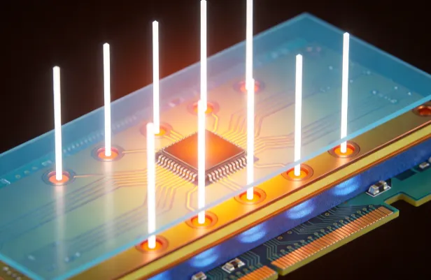
Wearable devices operate across temperature extremes, humidity ranges, and mechanical stress cycles that would be benign in consumer electronics but are aggressive in body-worn applications. The PCB material needs to maintain dimensional stability during reflow, resist delamination under thermal cycling, and provide consistent dielectric properties across the operating temperature range.
Standard FR-4 works for many applications, but wearables with demanding RF requirements or extended temperature specifications often need advanced laminates. Materials like Rogers 4350B, Isola I-Speed, or Panasonic Megtron 6 offer lower dissipation factors and tighter Dk tolerance than commodity FR-4, which translates directly to better RF yield and more predictable antenna performance.
The material decision cascades through the entire fabrication process. Different laminates have different drill characteristics, desmear requirements, and plating chemistries. A fabricator running high-mix, low-volume work needs to maintain process control across multiple material systems simultaneously—something that requires dedicated process development rather than parameter tweaking.
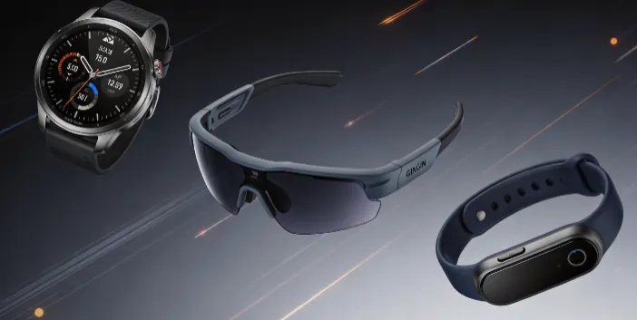
Wearable devices bend, flex, and experience impact loads that rigid consumer electronics never encounter. A smartwatch dropped on concrete, a fitness band twisted during exercise, AR glasses folded and unfolded repeatedly—these mechanical loads translate directly to stress on solder joints, vias, and interconnections.
HDI PCBs require careful attention to reliability in these applications. Microvias with high aspect ratios are more susceptible to barrel cracking under thermal cycling. Via-in-pad structures need proper fill and plating to prevent void-induced failures. The sequential lamination process itself introduces residual stresses that can affect long-term reliability if not managed correctly.
Qualification testing for wearable PCBs typically includes thermal shock (-40°C to +125°C), temperature humidity bias (85°C/85% RH), and mechanical shock specifications that exceed standard commercial requirements. Demonstrating reliability under these conditions requires both robust design margins and validated process controls—no amount of post-fabrication inspection can compensate for a fundamental process capability gap.
At WYD, we build dedicated HDI manufacturing workflows to serve wearable electronics developers. Our process engineers engage early in the PCB layout phase, providing practical DFM feedback to resolve potential manufacturability issues before prototype fabrication starts.
We maintain verified process qualifications for a wide range of substrate materials, including standard FR-4, Rogers, Isola and Panasonic high-frequency laminates. Both rigid-HDI and flexible-HDI (F-HDI) are supported to cover smart rings, AR glasses, fitness trackers and medical‑grade wearable sensors.
Our in-house reliability laboratory conducts standard qualification tests such as thermal shock, temperature-humidity bias and mechanical shock, replicating real-world operating stresses for body-worn devices. We maintain consistent stack-up configurations, material specifications and process parameters throughout prototype, DVT and mass-production stages, minimizing performance variation across different project phases.
From proof-of-concept samples to high-volume orders, our goal is to help customers balance product performance, yield, lead time and cost for wearable HDI PCB projects.
Miniaturized wearable devices push PCB interconnect technology to its limits. HDI PCB is not merely a way to shrink circuit features; it is a system‑level solution that reconciles high component density, signal integrity, thermal dissipation and long‑term mechanical reliability within ultra‑compact device housings.
Successful wearable product development depends not only on good schematic and layout design, but also on close alignment between design teams and PCB manufacturing partners. Early technical communication, reasonable material selection and rigorous reliability verification together lay the foundation for stable commercial‑grade wearable products.
Q1: Are HDI PCBs mandatory for wearable electronics? Can standard PCBs work as a substitute?
A: Standard PCBs are feasible for low density wearables with ample space and no high speed RF requirements. However, miniature products such as smart rings, AR glasses and continuous glucose sensors feature high component density and extremely compact board outlines. Constrained by trace and via capabilities, conventional PCBs cannot support such layouts, resulting in excessive board thickness or degraded signal performance. For these applications, HDI PCBs are mandatory.
Q2: Do HDI PCBs drastically increase the BOM cost of wearable products?
A: HDI carries higher intrinsic processing cost than traditional PCBs. Nevertheless, it may reduce layer count, shrink PCB footprint and simplify overall mechanical structure. Cost increments are more noticeable at the prototype stage; unit costs drop significantly at higher production volumes. Early DFM (Design for Manufacturability) optimization effectively controls expenses by avoiding unnecessary sequential lamination cycles.
Q3: For wearable HDI designs, should engineers prioritize FR 4 or high frequency laminates?
A: Standard FR 4 satisfies requirements for basic Bluetooth fitness bands and general purpose health monitors. AR glasses, TWS earbuds and devices requiring high bandwidth wireless transmission call for low loss high frequency materials such as Rogers or Panasonic Megtron 6. Material selection should balance RF specifications, operating temperature range and budget instead of blindly specifying premium substrates.