EN
EN
 it
it  fr
fr  de
de  ru
ru
Get in Touch with WeiYuanDa Now!


Modern smartphones are continuously decreasing in weight and thickness while simultaneously integrating advanced functionalities, including AI processing, multi-lens camera systems, 5G connectivity, and extended battery capacities. This increased functional density within a reduced form factor is primarily enabled by High-Density Interconnect (HDI) PCB technology. HDI micro-via engineering facilitates higher component integration in constrained spaces, which is a fundamental prerequisite for contemporary slim device architectures.
This article outlines the technical principles of HDI technology and its necessity in modern electronics. Furthermore, it details how WeiYuanDa PCB (WYD) applies advanced HDI manufacturing processes to provide compact, high-performance solutions for international OEMs.
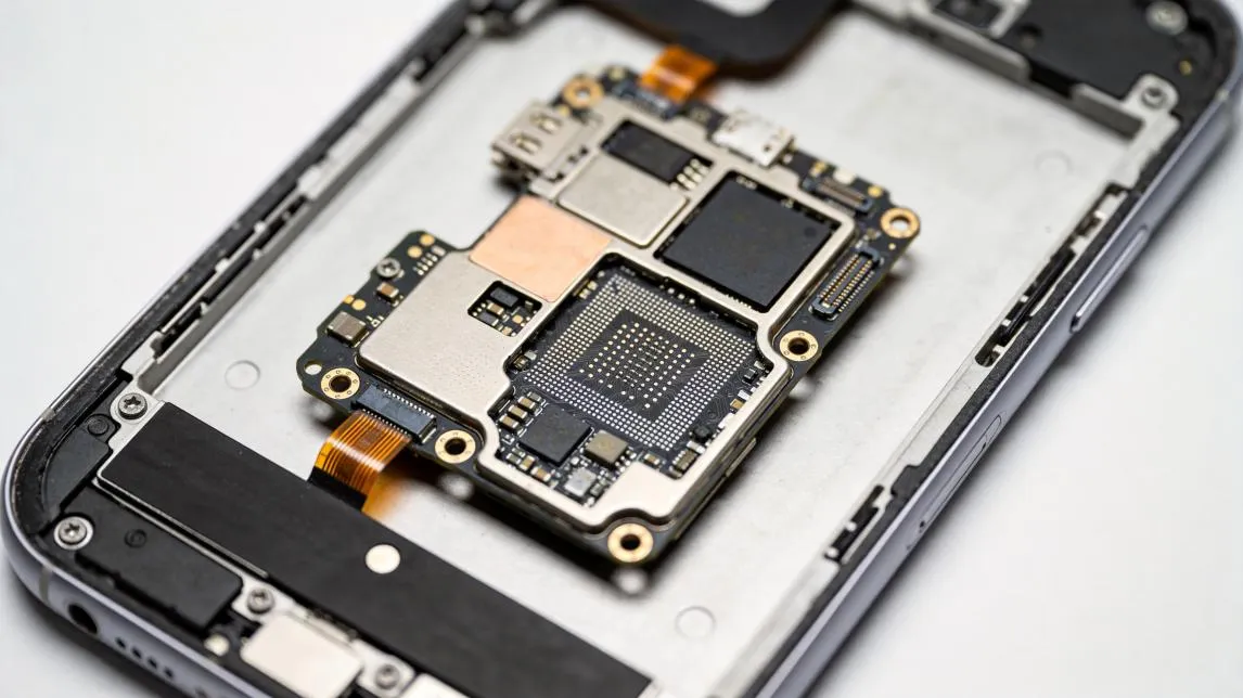
According to the IPC-2226 standard, an HDI (High-Density Interconnect) PCB is a circuit board characterized by a significantly higher wiring density per unit area compared to traditional PCBs. Its primary technical specifications at least include some of these:
Line width and spacing ≤ 100 microns.
Micro-via finished diameter < 150 microns.
Capture pad diameter < 400 microns.
Connection pad density exceeding 20 pads per square centimeter.
These features —finer lines, smaller micro-vias, and tighter spacing—enable a substantially higher circuit density within a reduced form factor. Consequently, this technology facilitates the development of electronic devices that are simultaneously more compact, lightweight, and high-performing.
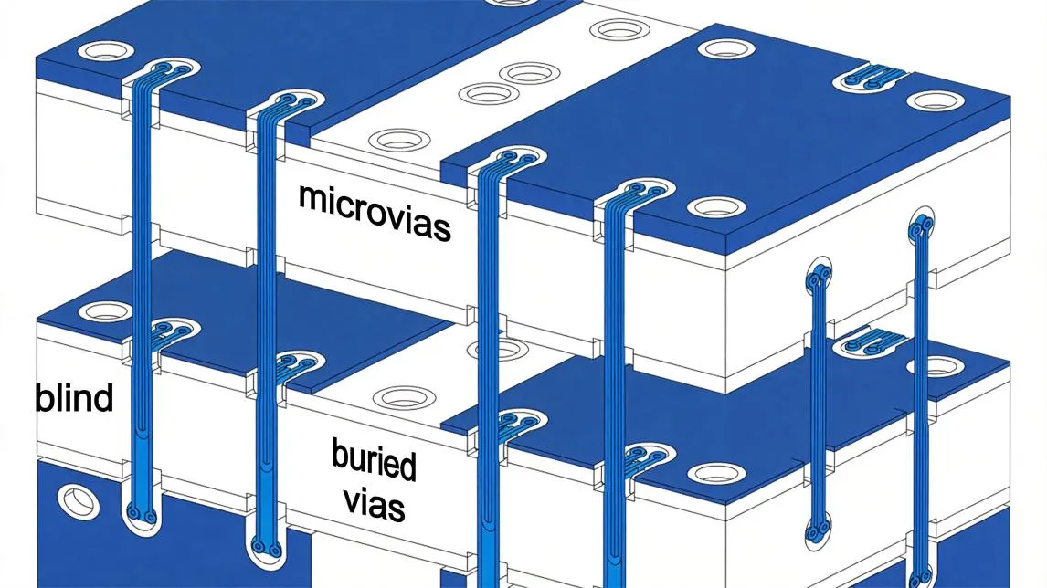
1. Laser-Drilled Microvias
Unlike traditional PCBs that rely on mechanical drilling, HDI utilizes laser drilling to create microvias with diameters as small as 0.10mm. This method enables efficient inter-layer connections while minimizing the consumption of valuable board space.
2. Sequential Lamination Process
HDI boards are constructed using a build-up process with multiple lamination cycles. This allows for complex interconnection structures, such as 1+N+1, 2+N+2, or 3+N+3 (where N represents the core layers), adding routing layers without increasing the board's overall footprint.
3. Fine Line and Space
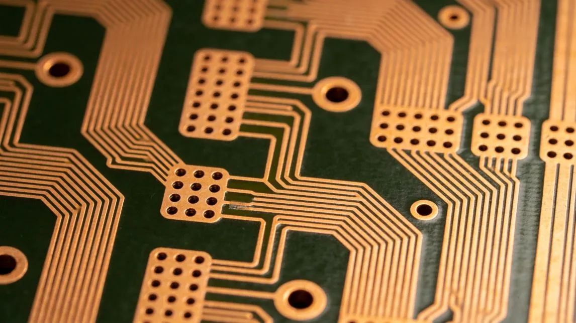
HDI technology supports line widths and spacing down to 2 mils (0.05mm) or finer. This high routing density is essential for accommodating high-speed signal interfaces like DDR5, USB 4.0, and PCIe 5.0 within compact designs.
HDI technology pushes line widths and spacing down to 2 mils (0.05mm) or even finer. This allows designers to route more signals in the same area, which is essential for high-speed interfaces like DDR5, USB 4.0, and PCIe 5.0.
While smartphones are the most visible application, HDI PCBs are everywhere in modern electronics:
Telecommunications and Data Centers: In equipment such as 5G base stations, high-speed routers, switches, servers, and optical modules, HDI PCBs are essential for ensuring high-speed data processing and transmission. They effectively manage high-frequency signals and reduce signal loss, thereby meeting the stringent requirements of high-performance chips, such as FPGAs and ASICs, for high-density routing and signal integrity. Consequently, they serve as a fundamental infrastructure supporting data flow in modern information systems.
Automotive Electronics: Driven by the advancement of vehicle intelligence and electrification, the application of HDI PCBs in automotive electronics is becoming increasingly critical. These PCBs are widely deployed in radar modules for Advanced Driver Assistance Systems (ADAS), in-vehicle infotainment systems, autonomous driving domain controllers, and Battery Management Systems (BMS) for new energy vehicles. Furthermore, these applications impose stringent demands on the reliability and environmental resistance (e.g., high temperature and vibration) of the circuit boards.
Medical Electronics: High-end medical diagnostic and monitoring devices rely on HDI PCBs to achieve high-precision acquisition and processing of weak physiological signals. Consequently, the high reliability of these PCBs is directly linked to overall equipment performance and patient safety.As devices become more intelligent and connected, the demand for HDI continues to grow across every industry that requires high performance in compact form factors.
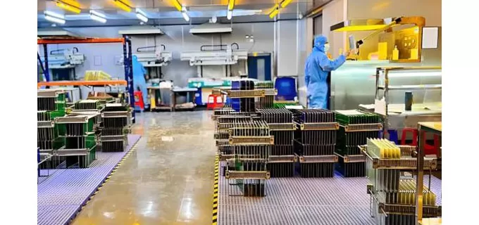
WeiYuanDa PCB (WYD) is a specialized HDI PCB manufacturer in China with a proven track record in delivering complex, high-mix, low-volume boards for global OEMs. Key manufacturing capabilities include:
Rapid Turnaround
WYD specializes in quick-turn HDI prototyping, supported by a dedicated engineering team available 24/7 with a guaranteed 24-hour response time. For expedited orders, single-layer boards can be delivered within 24 hours.
European Presence
To serve the European market efficiently, WYD operates a branch office in Modena,ITALY (WYD SRL). provides local technical support, sales coordination, and customer service, ensuring effective communication and optimized response times for European clients.
UL-Certified HDI Capabilities
WYD's HDI production is certified by Underwriters Laboratories (UL), ensuring compliance with international safety and performance standards. Furthermore, the company holds relevant certifications for medical devices, qualifying it as a reliable partner for healthcare applications.
High-Mix Low-Volume Expertise
Unlike mass-production facilities, WYD focuses on the manufacturing of complex, high-difficulty boards in small quantities, with a minimum order quantity (MOQ) of one piece. This capability is highly suitable for R&D centers, laboratories, and companies developing innovative products.
Q1: How fast can WYD deliver HDI prototypes?
A: For standard HDI prototypes, typical lead time is 7-10 working days counts after EQ / TQ / Working Gerber confirmation. Urgent orders can be accommodated with faster turnaround. Our engineering team is available 24/7 to support rapid project development.
Q2: Does WYD provide HDI design support?
A: Yes. WYD offers DFM (Design for Manufacturability) review services. Our engineering team can review your HDI design files and provide optimization suggestions to ensure manufacturability and reliability before production begins.
The next time you hold a slim smartphone or use a compact wearable device, remember that inside is an HDI PCB—a marvel of modern electronics engineering that makes miniaturization possible. Through laser-drilled microvias, sequential lamination, and fine-line routing, HDI technology enables more functionality in less space.
WeiYuanDa PCB combines advanced HDI manufacturing capabilities with rapid turnaround, UL certification, and dedicated support for global customers. Whether you're developing the next generation of smartphones, AI devices, or medical equipment, WYD has the expertise and capacity to bring your vision to life.
Ready to explore HDI PCB solutions?
Visit www.wyd-pcb.com or contact our team for a quote today.