EN
EN
 it
it  fr
fr  de
de  ru
ru  pt
pt  es
es
Get in Touch with WeiYuanDa Now!


As electronic products become smaller and more function-dense, traditional PCB layouts often struggle to provide enough routing space. Smartphones, AI devices, medical electronics, IoT modules, automotive systems, and telecom equipment all require more components, shorter signal paths, and stable electrical performance within limited board area. This is where HDI PCB technology becomes important.
An HDI PCB supports higher circuit density through microvias, finer lines, smaller spacing, and advanced layer structures. For engineers and OEM customers, understanding the HDI PCB definition, key HDI PCB design rules, and the HDI PCB manufacturing process can reduce project risk before prototype or mass production.
This revised version keeps the technical focus clear and reduces repeated supplier-selection wording.
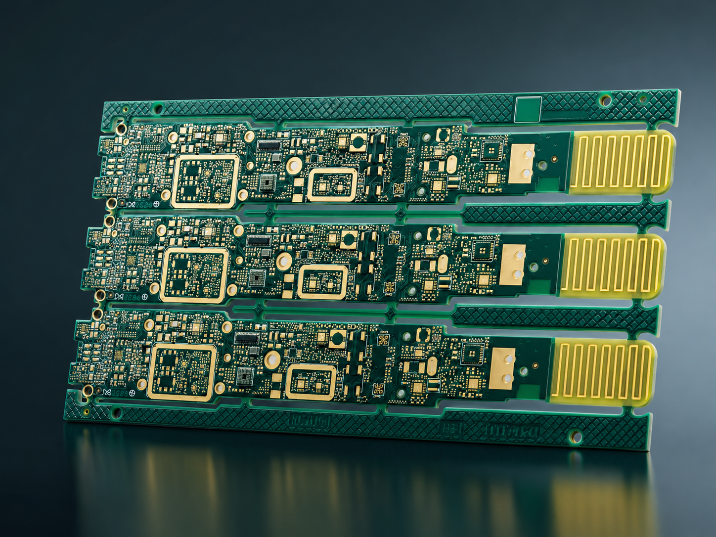
The basic HDI PCB definition is high-density interconnect printed circuit board. Compared with conventional PCBs, an HDI board uses finer circuit lines, tighter spacing, smaller vias, and higher connection density to place more electrical functions into a smaller area.
HDI technology is not only used to make a board smaller. It can also improve routing efficiency, shorten signal paths, support high-speed signal transmission, and make compact product structures possible. A typical HDI board may include microvias, blind vias, buried vias, via-in-pad structures, and sequential lamination.
HDI structures should be selected according to routing density, component package, signal requirements, board thickness, and production feasibility. Customers should not add advanced structures unless they solve a real layout or reliability problem.
HDI feature | Function | Typical use |
Microvia | Connects adjacent layers with a small laser-drilled via | BGA breakout, compact routing |
Blind via | Connects an outer layer to inner layers without passing through the full board | Routing flexibility and space saving |
Buried via | Connects internal layers only | Complex multilayer routing |
Via-in-pad | Places via inside component pad | High-pin-count chips and shorter routing |
Sequential lamination | Builds complex layer structures step by step | Advanced HDI and any-layer structures |
Good HDI PCB design is critical because HDI boards leave less room for design mistakes. Traces are thinner, spacing is tighter, and vias are smaller, so the design should be checked before production.
· Confirm minimum line width and spacing against manufacturer capability.
· Check microvia size, depth, aspect ratio, and pad design.
· Review BGA escape routing and via-in-pad requirements.
· Plan impedance-controlled traces before finalizing layer stack-up.
· Balance copper distribution to reduce lamination and warpage risk.
· Leave enough solder mask bridge and assembly clearance where possible.
Compact electronics often generate heat in a small area. While HDI is mainly associated with density and routing, thermal behavior should still be considered. Component placement, copper distribution, ground planes, thermal vias, and stack-up design can affect how heat spreads through the board.
Signal performance is another reason why HDI PCB design matters. Shorter interconnection paths can help reduce signal loss, delay, and unwanted interference in high-speed circuits. For products involving data processing, wireless communication, sensors, or RF functions, layout planning has a direct impact on stability.
The HDI PCB manufacturing process requires higher precision than standard PCB production. A stable process usually starts with DFM review, where the manufacturer checks stack-up, line width, spacing, via structure, copper thickness, material selection, and surface finish.
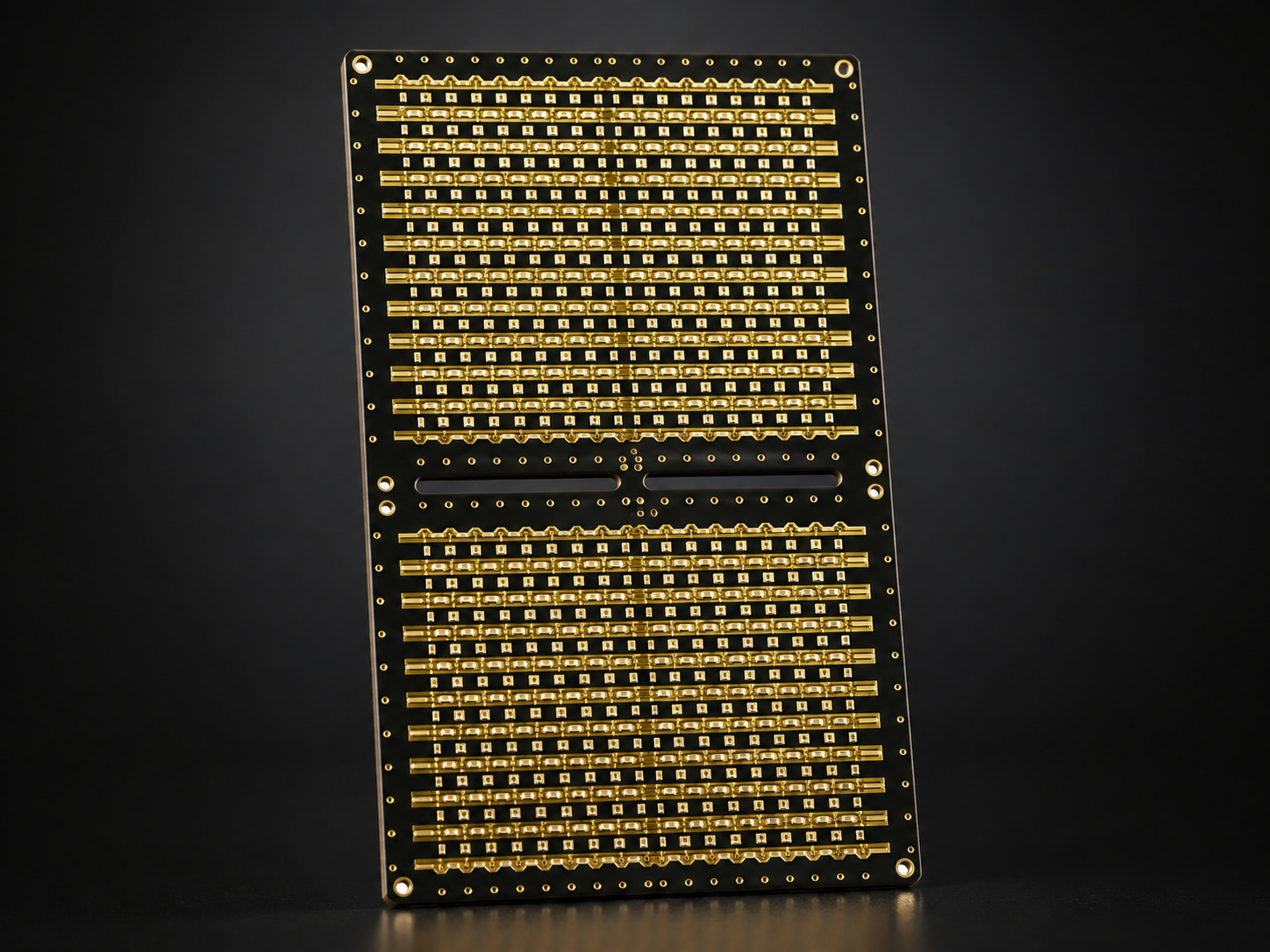
Laser drilling is a key step because microvias are much smaller than standard drilled holes. After drilling, plating and filling processes build reliable electrical connections. Some HDI boards also require sequential lamination, where layers are built in multiple cycles to form complex interconnection structures.
After lamination and via formation, the board goes through imaging, etching, surface finish, electrical testing, and final inspection. Surface finish options such as ENIG, OSP, HASL-LF, immersion tin, immersion silver, or gold finger may be selected according to assembly and reliability needs.
Actual capability may vary depending on stack-up design, material selection, application requirements, and final engineering review.
Parameter | Standard HDI | Advanced HDI |
Layer Count | Up to 24 Layers | Up to 32 Layers |
Material | FR-4 TG170 | Rogers 4350, 370HR |
Laser Via Size | 0.15 mm | 0.20 mm |
Min Line / Space | 3 mil | 2 mil |
Aspect Ratio (Laser Via) | 1:1 | 0.8:1 |
Surface Finish | HASL / ENIG / OSP | HASL / ENIG / OSP |
With more than 20 years of PCB manufacturing experience, WEIYUANDA PCB supports Multilayer HDI PCB, High-Frequency PCB, and IMS PCB projects with a focus on quality control, on-time delivery, and rapid engineering support.
For HDI PCB projects, customers can share Gerber files, stack-up requirements, material preferences, impedance requirements, surface finish needs, expected application, and production volume for engineering review. This helps identify layout risks, stack-up problems, microvia concerns, material limitations, and mass production challenges before they affect delivery.
To learn more about WEIYUANDA's HDI PCB manufacturing capabilities, you can share your stack-up, Gerber files, application requirements, and delivery needs with the WEIYUANDA PCB team for engineering review and project support.
Understanding the HDI PCB definition is the first step, but successful HDI projects require more than knowing what HDI means. Customers also need to understand how HDI PCB design affects routing density, signal performance, thermal behavior, and manufacturability.
For compact electronics, high-speed circuits, AI devices, medical electronics, IoT modules, and telecom systems, HDI PCB technology can fit more functions into less space while supporting stable performance. Early DFM review with an experienced manufacturer can reduce rework and improve the transition from prototype to mass production.