 EN
EN
 it
it Standard HDI PCB
Ideal for consumer electronics, with 4-8 layers and microvias for compact, cost-effective designs.


At WeiYuanDa PCB, we specialize as a leading HDI PCB factory in China, delivering compact, high-performance HDI PCB boards for demanding applications. Our advanced high-density interconnect HDI PCBs with microvia technology ensure superior reliability, faster signal transmission, and efficient space utilization, making them ideal for smartphones, AI systems, and medical devices. As a trusted HDI printed circuit board supplier, we provide rapid HDI PCB prototyping, consistent quality, and competitive solutions tailored to global OEMs.
Partner with WeiYuanDa PCB today to accelerate your product development with proven manufacturing expertise.
| Parameter | Standard HDI | Advanced HDI |
| Layer Count | 24 Layers | 32 Layers |
| Max PCB Size | 300mm*450mm | 400mm*500mm |
| Raw Material | FR-4 TG 170 | Rogers 4350, 370HR |
| Outer Based Cu | 1OZ | 2OZ |
| Inner Based Cu | 1OZ | 2OZ |
| Aspect Ratio (PTH) | 12:01 | 15:01 |
| Aspect Ratio (Laser) | 1:01 | 0.8:1 |
| Surface Treatment | HASL, ENIG, OSP, Gold Finger, Immersion Tin, Immersion Silver | HASL, ENIG, OSP, Gold Finger, Immersion Tin, Immersion Silver |
| Laser Hole Size | 0.15mm | 0.2mm |
| Min Line/Spacing Outer | 3 mils | 2 mils |
| Min Line/Spacing Inner | 3 mils | 2 mils |
| Solder Mask Bridge | 5 mils | 3 mils |
| Via Hole | 20 mils | 8 mils |
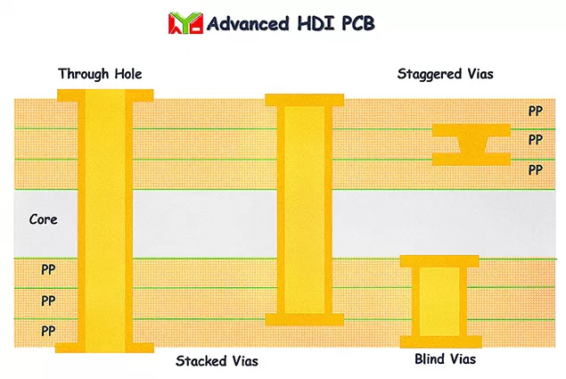
HDI PCB Definition: HDI PCB, or High-Density Interconnect Printed Circuit Board, according to the IPC-2226 standard, is a type of circuit board with a wiring density that far exceeds traditional PCBs per unit area. Its key features include:

High-Density Design
Line width and spacing <100 microns, microhole diameter <150 microns
Pad diameter <400 microns
Pad density exceeding 20 per square centimeter

Multi-Layer Structure
Common layer count ranges from 4 to 22 layers
Advanced designs can reach up to 30 layers

Microhole Technology
Laser drilling is used, with microhole diameters <0.15 mm, aspect ratio 1:1, depth <0.25 mm
Supports blind and buried hole structures (e.g., 1+n+1, 2+n+2, 3+n+3)

Material and Process
Uses FR4 standard, high-performance FR4, eco-friendly FR4, or Rogers materials
Surface treatments include OSP, ENIG, and tin immersion

Design and Layout: Using advanced PCB design software, we optimize routing and apply Laser Direct Imaging (LDI) to directly print circuit traces, improving accuracy and production efficiency.
Material Selection: We carefully choose low dielectric constant materials such as standard FR4 (IT-158, IT-180), high-performance FR4 (Isola 370HR, Ventec VT-47), eco-friendly FR4 (Shengyi S1000-2M, Kingboard KB-6160), or Rogers laminates (4350B, 4003C). Our large inventory of Rogers materials supports fast delivery for high-frequency and high-performance applications.
Laser Drilling: Precision laser drilling machines create microvias with diameters under 0.15 mm, aspect ratios of 1:1, and depths less than 0.25 mm—essential for HDI PCB board designs requiring compact interconnections.
Sequential Lamination: Through advanced lamination technology, multiple layers are bonded with prepreg under controlled temperature and pressure, ensuring accurate layer-to-layer alignment in HDI printed circuit boards.
Plating and Etching: Copper is deposited on hole walls and circuit paths, followed by precise chemical etching to form clean and stable conductor patterns.
Surface Treatment: We apply finishes such as OSP, ENIG, or tin immersion to protect copper traces, enhance solderability, and guarantee long-term performance.
As a professional HDI PCB manufacturer in China, WeiYuanDa PCB follows a strict and advanced process to deliver reliable high-density interconnect PCB boards. Each step is carefully controlled to ensure precision, durability, and consistency for global OEMs.
Miniaturized Design: HDI PCB boards greatly reduce the size and weight of devices, making them the ideal choice for smartphones, wearables, and other portable products.
Excellent Signal Integrity: With low signal loss and stable transmission, high-density interconnect PCBs ensure superior performance in high-speed and high-frequency applications.
High Component Density: By integrating more functions into limited space, HDI PCBs minimize the need for multiple layers, enabling compact and efficient designs.
Enhanced Reliability: Built to withstand heat, vibration, and demanding conditions, HDI printed circuit boards deliver long-term stability and consistent performance.
Cost-Effectiveness: Although initial production costs may be higher, optimized system design reduces overall expenses, making HDI PCBs a cost-efficient solution for advanced projects.
These combined advantages make HDI PCBs the preferred technology for industries requiring high performance, durability, and miniaturization.

Standard HDI PCB

Advanced HDI PCB

Ultra HDI PCB

Standard HDI PCB
Ideal for consumer electronics, with 4-8 layers and microvias for compact, cost-effective designs.


The ongoing miniaturization of electronic components is driving printed circuit boards toward levels of complexity that were unimaginable just a few years ago. Modern devices demand more functionality and higher performance, all within thinner and lighter HDI PCB boards. Achieving this requires a rigorous design approach and precise HDI manufacturing process.
As high-density interconnect PCBs evolve, narrower routing spaces lead to thinner traces, smaller gaps, and microvias with extremely small diameters. To meet these challenges, specific design solutions are applied:
Blind vias: laser-drilled holes on external layers
Buried vias: laser-drilled holes connecting internal layers
Advanced materials: thinner pre-preg and CCL laminates compared to conventional multilayer products
When designs reach such extremes, it is essential to follow strict design guidelines and collaborate closely with an experienced HDI PCB supplier like WeiYuanDa PCB. This ensures reliable performance, manufacturability, and faster time to market.


")